Because printed circuit boards have a wide range of use cases and applications, they require different techniques and technology to produce them. The most important feature of the PCB is its connectivity. There are many ways to form connections on a circuit board during the assembly process. One of the most popular is using press-fit technology. This guide will explore what it is and the pros and cons of using it. Additionally, it will examine how you can integrate it into your assembly process.
Contents
What is Press Fit Technology?
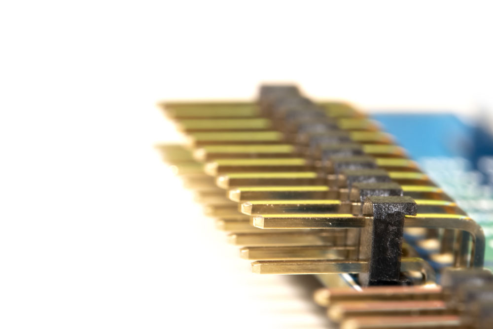 Press-fit electronic connector pins on circuit boards
Press-fit is a solderless technology that allows you to form electrical-mechanical interconnections between PCBs and components. During the press-fit process, a machine or technician pushes a pin into the thru-hole plating of the PCB.
Next, the manufacturer cold-welds the contact points between the press pins and the walls of the thru-hole plating. The cold-welding process creates gas-tight zones.
Using this technology may be preferable to thru-hole and surface mount technology because it creates highly reliable connections. Furthermore, it can help manufacturers avoid placing thermal stress on the PCB during the assembly process largely because it doesn't require soldering.
Incorporating press-fit is generally a straightforward process. As such, manufacturers can potentially utilize it in nearly any contact-to-PCB interconnections. However, most tend to use them in unique productions.
Advantages of Press-Fit Technology
Some of the press-fit technology's key benefits include:
- Allows you to create interconnections with common failures in time (FIT) rates.
- It can result in low revision rates and faster production times because it does not require soldering.
- Helps manufacturers avoid soldering-related defects such as flux residuals, solder balls, cold solder joints, etc.
- Does not require heating of the headers and thus, helps avoid thermal expansion.
- It is a more environmentally friendly solution compared to soldering because it does not require as many chemicals during the production and assembly process.
- This can result in cost savings and quality improvements for older designs.
Press Fit Tolerance
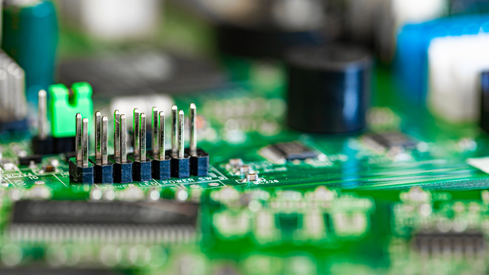 Connector pins on PCB
Mechanical engineering requires components to either easily slip together or permanently fit together. Press-fit falls into the second category. When manufacturers design PCBs, they use a set of dimensions and measurements. Often, the dimensions of the final product deviate from the initial plan.
Press-fit connections can have both bilateral and unilateral tolerance. Tolerance describes how much the final product can deviate from the plan and remain functional. We can see it as "room for error."
Special Offer: Get $100 off your order!
Email [email protected] to get started!
Calculating Press Fit Force and Pressure
When using a machine to apply pins to a PCB, it's important to understand the force required to properly engage and disengage the fixtures. We can use the following formula to calculate the minimum force a machine requires to apply and possibly remove the pins:
F = μ x pmax x A
μ: Describes the friction between the pins and the wall of the plated through-holes
pmax: Refers to the pressure between the pins and the walls of the plated through-holes
A: Refers to the area of contact between the pin and the walls of the plated through-holes
You can calculate the generated pressure between the pins and the walls of the plated through-holes on the PCB by dividing the force by the area (p = F/A).
The equation can be a little overwhelming and hard to understand. Thus, we have included a link to an excel sheet containing a set of example figures and measurements. You can use this excel sheet to calculate the force required by adjusting some of the measures and figures. Additionally, it will also help you calculate the area of contact.
Note: Shaft refers to the pin. Hub refers to the walls of the through-hole plate.
You can calculate maximum transmittable force (deliverable without slip) using the following formula:
T = F x d ÷ 2
F: Refers the maximum force required to engage and disengage the pins
d: Refers to the diameter of the pin (shaft)
Types of Press-fit Pins
There are two main types of press-fit pins. The first has a solid press-in zone. Essentially, this type of pin has low tolerance but high stability. The second is the elastic press-in area pin. It has a higher tolerance factor and is more compliant.
Press Fit Pin Material
The pins typically consist of three different sections. These sections include a top plating that acts as a finish, underplating for protection, and base material for the foundation.
Each section of the pin uses different materials. However, this composition may depend on the processor PCB manufacturer. Nevertheless, here is a breakdown of all the materials we use to construct pins ordered by section:
- Top plating: Pure Tin (Sn)
- Underplate: Pure Nickel (Ni)
- Base material: Tin reinforced copper alloy (CuSn4), Phosphor bronze copper alloy (CuSn6), Precipitation-hardened copper alloy (CuNisi), High-Performance Copper (CuCrAgFeTiSi)
When to Use Press Fits in Your Assemblies?
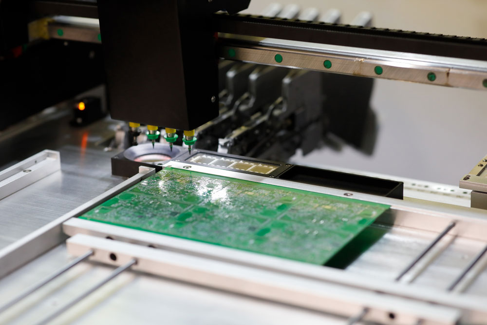 Automatic pick and place machine for PCB assembly
When deciding if using this technology is worth incorporating into your design or assembly process, you need to consider a few things. For instance, using pins may not suit massive productions, even with automated press-fit assembly processes.
Furthermore, finding and installing suitable machines and fixtures may increase production costs, mainly if you use a custom-stamped press-fit configuration. However, this technology is ideal for miniaturized circuitry and modularization. It's also highly reliable and can cut down on some material costs.
Is Press-Fit's Permeant?
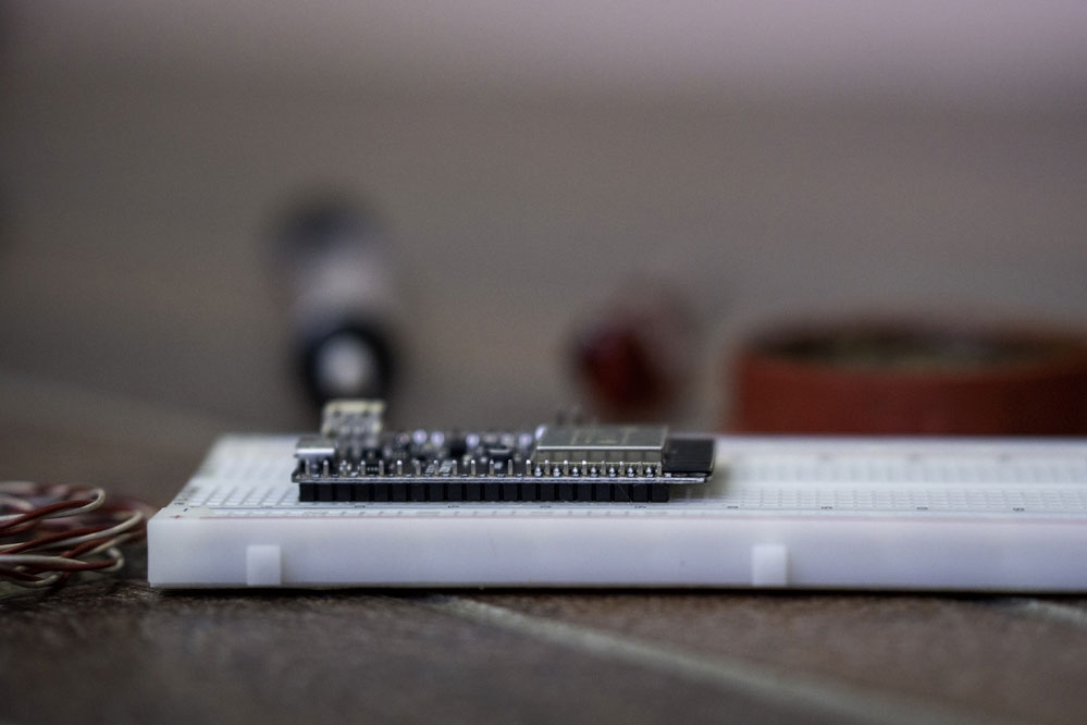 Microcontroller with press-fit pins connected to the breadboard
Much like soldering, we can use press-fit to form permanent connections. However, we must ensure that our measurements are correct when engaging the pins into the through-holes. This process relies primarily on stress and friction.
If the fit is tight enough, pins should be able to build permanent bonds. However, if there isn't enough friction or stress between the plug and the through-hole walls, the nail may not be able to sustain enough pressure to stand on its own or maintain a lasting bond.
Conclusion
The above guide explored press-fit technology for PCBs. Furthermore, it discussed if it is a viable alternative to conventional mounting technology such as SMT and THT. We can conclude that there are many benefits of press-fit, and thus, it's here to stay. Nevertheless, when selecting a manufacturer to produce your press-fit PCB designs, choose a reputable PCB fabricator. This method is the best way to ascertain the quality and longevity of your products.
Special Offer: Get $100 off your order!
Email [email protected] to get started!


