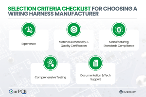
Top 10 Classic Car Wiring Harness Manufacturers | Full Guide
Finding the right wiring harness manufacturer for your vintage ride can be a real headache. Those beautiful old machines need special wiring that looks period-correct


We at OurPCB are here to assist you. Our PCB prototype service offer up to 50 layers, available in 5, 10, and 20 units. As a leading PCB manufacturer with lots of happy customers all around the world, especially in the USA, our team of experienced professionals is dedicated to delivering high-quality, reliable PCB Assembly services to meet all your electronic requirements.


A specific grade of combined fiberglass and reinforced epoxy laminate.
A synthetic polymer, known for its high tensile strength, flexibility, and durability.
A family of high-performance laminate materials.
Made of woven glass fabric surfaces and a non-woven glass core, bonded together with an epoxy resin binder.
Used in conductive traces and planes, as well as heat management.
A dielectric material used to bind and insulate the copper layers within a multilayer PCB.
OurPCB is a leading PCB assembly manufacturer, in the industry, and we’ve been providing PCB prototype services for almost 20 years. We offer small quantity circuit board prototyping to help you test and validate your product before going to market, without breaking the bank.
We’ve provided services for over 3,000 happy PCB customers to date. Once your PCB prototype has been validated, we’re here to help you move to full production at a cost-effective price and get your product to market as soon as possible.
| Quantity: 5 | 50 cm² | 100 cm² | 200 cm² | 400 cm² | 600 cm² |
|---|---|---|---|---|---|
| 1-Layer | $17 | $21 | $26 | $36 | $46 |
| 10-Layer | $259 | $279 | $308 | $359 | $412 |
Your final cost will depend on how many PCB prototypes you need. Request a free online pcb quote for your prototype project now. New customers get $100 off their first project with us!
| Number of Layers | Number of Days |
|---|---|
| 1-12 layers | within 72 hours |
| 12+ layers | within 120 hours |
Lead time may extend depending on the quantity of PCB orders. Contact us today for a free quote to get an accurate estimation of the lead time you can expect.

Provide us with your Gerber file for a custom quote.
Our experts will analyze your design and suggest changes if necessary.
We’ll send you a final quote for approval before we go ahead with the production process.
Once approved, we’ll begin manufacturing your PCB prototype.
Our rapid turnaround services and our trusted courier partners will get you your sample in record time.
| Quantity: 5 | 50 cm² | 100 cm² | 200 cm² | 400 cm² | 600 cm² |
|---|---|---|---|---|---|
| 1-Layer | $17 | $21 | $26 | $36 | $46 |
| 10-Layer | $259 | $279 | $308 | $359 | $412 |
Your final cost will depend on how many PCB prototypes you need. Request a free online pcb quote for your prototype project now. New customers get $100 off their first project with us!
| Number of Layers | Number of Days |
|---|---|
| 1-12 layers | within 72 hours |
| 12+ layers | within 120 hours |
Lead time may extend depending on the quantity of PCB orders. Contact us today for a free quote to get an accurate estimation of the lead time you can expect.
Provide us with your Gerber file for a custom quote.
Our experts will analyze your design and suggest changes if necessary.
We’ll send you a final quote for approval before we go ahead with the production process.
Once approved, we’ll begin manufacturing your PCB prototype.
Our rapid turnaround services and our trusted courier partners will get you your sample in record time.
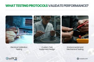
A prototype is the ideal way to detect and fix errors before full-scale production. Creating and testing a batch of 5 to 20 products is much more cost-effective than producing hundreds or thousands without realizing there’s a flaw. Addressing these issues early prevents performance problems and ensures the final product meets quality standards.
Prototyping allows engineers to validate the design and ensure all components interact correctly. Any discrepancies between expected and actual behavior can be identified and resolved early. This process optimizes functionality, reduces the risk of defects, and improves overall product reliability.
Fixing errors at the prototype stage speeds up production. Even going through several iterations of prototype PCBs is faster than discovering flaws during large-scale manufacturing. A streamlined development process allows businesses to launch their products sooner and start generating revenue faster.
By catching errors early, prototypes help prevent costly mistakes in mass production. Fixing issues at this stage is much cheaper than recalling and reworking faulty products later. While multiple iterations may seem like an extra cost, they ensure high-quality, optimized products that perform reliably under real-world conditions.
Low-volume prototype PCB production allows for quick design modifications without wasting valuable time or resources. Engineers can refine product features, test new ideas, and make necessary adjustments on the go. This flexibility enhances innovation and ensures that the final product meets market demands.
Taking the time to prototype and optimize before going to market gives companies a competitive edge. Businesses that prioritize quality over speed can avoid costly mistakes, build a better reputation, and allocate savings toward marketing or product enhancements. In a competitive industry, early testing and refinement can be a game-changer.
Mon-Fri: 24 hours,
Sat: 9am-6pm, GMT+8
Reach us at
[email protected]
24 hours online
+86-199-30589219
Mon-Fri: 24 hours,
Sat: 9am-6pm, GMT+8
PCB prototyping is the process of creating a preliminary version of a printed circuit board to test its functionality and design. This prototype allows engineers to identify and rectify any issues before the final production run.
After prototyping, the next steps typically include:
Finding the right wiring harness manufacturer for your vintage ride can be a real headache. Those beautiful old machines need special wiring that looks period-correct
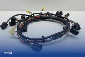
Would your car be able to run without wire harnesses? Not a chance. Wire harnesses connect all the electrical parts together. No harness means no
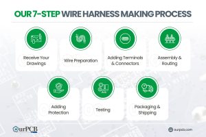
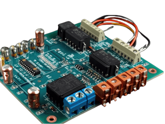
Making wire harnesses isn’t complicated. At OurPCB, we create custom wire harnesses for an expansive range of industries every day. While it’s a complicated process,
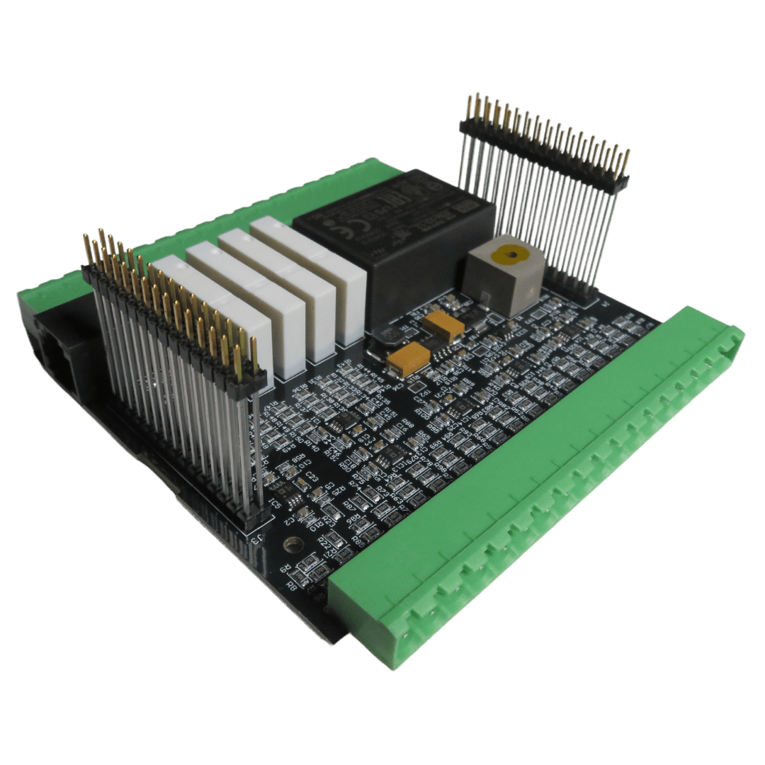
Prototype cable assemblies are the very important place in between PCB design ideas and interconnects. OurPCB brings prototype assemblies with PCB solutions to your tables.
PCB thermal management prevents component overheating through strategic heat transfer techniques. Without proper thermal control, electronics are at risk of electronic failures through weakened solder
ContentsKey TakeawaysWhat is a Multilayer-Printed Circuit Board?How do Multilayer PCB Boards Work?Multilayer PCB ApplicationsMultilayer PCB Manufacturing Process: StepsMultilayer PCB Manufacturing MachinesBenefits of Multilayer Circuit BoardsWhat
We use cookies to improve your browsing experience, which may include personal information. By clicking "Agree," you accept our Privacy Policy and cookie use. You can change your cookie settings in your browser anytime.
Agree
 Chat With Us
 Free Quote