Contents
- Types of Flexible PCBs
- Advantages of Flexible PCBs
- Disadvantages of Flexible PCBs
- Applications of Flex PCBs
- Flexible PCB Manufacturing Process
- Flexible Laminate and Copper Fabrication and Lamination
- Drilling and VCP Electroplating
- Circuit Transfer
- Etching
- Positioning Hole Drilling
- Electrical Testing
- Cleaning and Scrubbing
- Layer Alignment and Lamination
- Silkscreen Printing and Baking
- Surface Finish Application
- Finished Board Electrical Testing
- Profiling
- Visual Inspection
- Sample Testing for Quality Control
- Packaging and Storage
- Flex PCB Design Considerations
- Where to Buy Flex PCBs
- The Bendability of Flex PCB
- Flex PCB Prototype Correct Thickness
- Typical Flexible PCB Schematic Diagram and Stackup
- Single Layer Flex PCB
- Double Access/Back Barred FPCB
- Double Layer FPCB
- Multi-Layer Flex PCB
- Materials Used in Flex Circuits
- Flexible PCB Design: How To Design Flex Circuits
- Custom Flex PCB: Why Use Stiffeners in Flex Circuit Applications
- Rigidizing Connector and Component Stiffeners
- ZIF Stiffeners
- Localized Bend Constraints
- Factors Affecting the Cost and Turn-Around Time of Your Flex PCB
- IPC Standards for Flexible Circuit Board Manufacturing
- How To Choose a Flex PCB Manufacturer
- OurPCB: A Leading Flexible PCB Manufacturer
Types of Flexible PCBs
| Type of Flexible PCB | Description |
|---|---|
| Single-Sided Flex PCBs | These printed circuit boards (PCBs) have a single layer of conductive material on one side of a flexible dielectric layer (such as polyimide or polymer film), making them simple and versatile. |
| Double-Sided Flex PCBs | These feature a flexible dielectric material with a conductive copper layer on both sides. Metalized holes connect the copper layers for signal transmission. |
| Multilayer Flex PCBs | These multilayer PCBs have multiple layers of copper traces separated by flexible dielectric layers, allowing for more complex circuitry in compact spaces. |
| Rigid-Flex Circuits | These combine rigid and flexible PCB layers into a hybrid structure, offering high circuit density while maintaining flexible sections for dynamic applications. |
| HDI Flexible PCBs | High-Density Interconnect (HDI) flexible PCBs use thin, flexible substrates to support multiple electronic components, enabling better performance in compact designs. |
| Sculptured Flex Circuits | These flexible circuits have varying copper thickness throughout their design, allowing for areas with enhanced strength or conductivity as needed. |
| Polymer Thick Film Flexible PCBs | Polymer thick firm use flexible polymer films and stencils for screen printing conductive traces, offering an affordable solution for low-voltage applications. |
| Double Access/Back Barred Flex PCBs | These special single-sided flexible PCBs provide conductive track access from both sides, achieved through pre-punched dielectric films and strategic etching. |

A flex PCB. See how it takes up less space when folded or rolled.
Advantages of Flexible PCBs
- Save space and weight.
- Increased stability and reliability
- Eliminates the use of connectors and wire harnesses and minimizes wiring errors
- Possible to stack them in various configurations
- High tensile strength & high resistance to radiation, chemicals, and extreme temperatures
- Durable (ideal for harsh environments)
- Easy to install
- Delivers a strong signal quality
- Improves impedance control
Disadvantages of Flexible PCBs
- It has a higher cost compared to rigid PCBs in specific applications
- It uses a complex assembly process
- Difficult to repair or rework
- Needs proper storage conditions
- Easily damaged through improper handling
Applications of Flex PCBs
- High-speed digital/RF/microwave connectors
- Industrial sensors. Understand the different types of sensors used in industrial applications
- Instrumentation consumables
- Medical devices - wearables
- Automotive
- Satellites
- Avionics
- Consumer electronics
Flexible PCB Manufacturing Process
Flexible Laminate and Copper Fabrication and Lamination
This process involves brushing the PI film with adhesive and laminating it to form the overlay.
The copper foil also gets pressed to the required thickness for the board. These two layers are mated to make the overlay laminate the copper foil.
Drilling and VCP Electroplating
Drill holes through the copper layer to connect them if the board has two or more.
These holes are electroplated using copper on the vertical continuous plating line to create an even PTH thickness.
Circuit Transfer
The copper laminate gets a UV-sensitive photoresist layer printed above it, then a film of the circuit’s negative image is placed above this laminate and the copper gets exposed to UV light.
Etching
The etching machine uses a sodium hydroxide solution to dissolve the areas with the uncured photoresist layer. After that, this machine washes away the cured photoresist layer.
Positioning Hole Drilling
A mechanical drill bores three positioning holes diagonally on the board.
Electrical Testing
This testing process evaluates the electrical performance of the etched circuit using a power-on self-test.

A circuit board undergoing flying probe testing
Cleaning and Scrubbing
Cleaning removes the residual sodium hydroxide, metal oxides, and moisture, while scrubbing makes the surface glossy.
Layer Alignment and Lamination
This step aligns the copper and overlay layers before exposing them to high temperatures.
Silkscreen Printing and Baking
The silk screen printing machine places the required logos, marks, and symbols on the board; then the silkscreen undergoes baking to dry the layer.
Surface Finish Application
Protect the copper pads from oxidation using a surface finish like ENIG.
Finished Board Electrical Testing
This second electrical test checks the integrity of the circuit after lamination and silkscreen printing.
Profiling
Profiling means cutting the edge rails to separate the individual boards on the production line.
Visual Inspection
Experienced technicians inspect the complete flexible boards visually to check for scratches and contamination. They also count the boards to check if the production quantity is correct.
Sample Testing for Quality Control
The last testing step involves picking a sample of up to 10% of the manufactured flex PCBs randomly from the produced batch for testing.
Packaging and Storage
Once manufacturing and testing are complete, the fabricator should package the flex board batches according to your requirements and keep them in a warehouse before delivery.
Flex PCB Design Considerations
- Layout Guidelines: Careful placement of components and routing of traces to minimize stress and ensure flexibility.
- Stack-up Design: Optimizing the layer arrangement and dielectric thickness to achieve the desired electrical and mechanical properties.
- Thermal Management: Incorporating features to dissipate heat and prevent thermal issues.
Where to Buy Flex PCBs
China is the world's largest producer of PCBs, with manufacturers offering a wide range of services from PCB design and fabrication to assembly.
| Manufacturer | Services Offered | Certifications | Specialization | MOQ | Lead Time (Prototypes) |
|---|---|---|---|---|---|
| OurPCB | Design, Fabrication, Assembly |
|
Complex, High-Performance PCB Production | Flexible | 1-3 Days |
| JLCPCB | Fabrication, Assembly, Prototyping | ISO 9001 | Fast Turnaround, Low-Cost Production | No MOQ | 1 Day |
| XPCB | Rigid, Flex, RF, Multilayer PCBs | ISO 9001 | Multilayer, HDI, Rigid-Flex PCBs | Flexible | 2-5 Days |
| Viasion | Low-Medium Volume Fabrication, Assembly | ISO 9001, UL | RF & Microwave PCBs, Up to 40 Layers | Small Batches | 5-10 Days |
| PCBMay | Design, Fabrication, Assembly | ISO 9001, IPC Class 2 & 3 | Aerospace, Telecommunication, Railways | No MOQ | 3-7 Days |
Special Offer: Get $100 off your order!
Email [email protected] to get started!
The Bendability of Flex PCB
Flexible PCBs can bend, but there is a limit to how many times you can bend them and the extent to which they can flex.
When you consider the number of times it can bend, static boards can only flex 100 times or less because manufacturers consider them as bend to install.
In most cases, you’ll only bend them during PCB assembly, leaving a big allowance of flex cycles to play with later during repairs or maintenance.
But dynamic PCBs can withstand thousands or tens of thousands of bends because they flex regularly.
The primary factor that determines this level of flexibility is the material thickness. The thinner the board, the more pliable it will be and the more flexing cycles it will handle.
When considering the extent to which they can bend, we’ll look at the bend radius.
You can determine the minimum angle at the flexible region can bend early on during PCB design.
Flex PCB Prototype Correct Thickness
You can determine the most suitable flexible PCB thickness of the prototype circuit by considering several factors in the equation.
For instance, PCB weight is a significant aspect because heavy materials are stiffer, but they have some performance benefits.
Light materials are cheaper and more flexible, but they usually have lower heat dissipation properties and high dielectric constants.

A flexible PCB with a chip and some components soldered onboard
If your board needs hot active components, you must use stiffeners, or the entire circuit must be on a thick substrate to hold heat sinks. Similarly, boards that require chips like microcontrollers and microprocessors must have stiffened areas to accommodate both active and passive components effectively. For those looking for a cost-effective solution, a DIY heatsink can be an excellent option to manage heat effectively.
However, thick PCBs require more materials to fabricate the layers, which increases manufacturing cost per square foot.
Reliability is also critical, and the determining factor is the board's thickness.
Thin boards are more flexible than thick ones, which makes them more reliable because they have a larger bend radius and can withstand more flex cycles.
Generally, circuit boards with a thickness of less than 1 oz./sqft are the most flexible and reliable if the application is in a flexible environment.'
Typical Flexible PCB Schematic Diagram and Stackup
A flex PCB consists of several layers, but the number varies depending on the type. These structure diagrams and stack-ups can help you during the design process when building one.
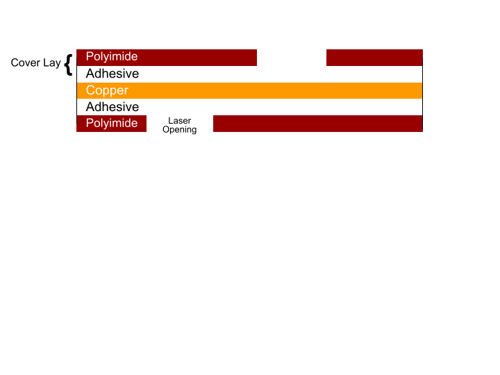
Single Layer Flex PCB
Single-layer FPCBs have a simple stack-up that comprises a flexible base layer (usually polyimide), then an adhesive layer followed by copper. A protective layer (cover lay) consisting of an adhesive and polyimide covers the metal. However, the conductive part cannot be left exposed.
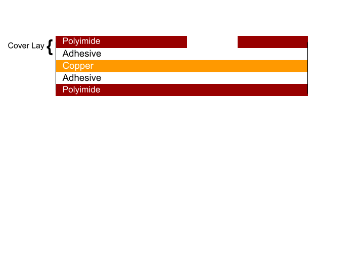
A single-sided flex PCB
Double Access/Back Barred FPCB
Like the single-layer electrical circuit, this one has five layers but with one difference. The polyamide outer layer on the base has a laser opening to access the copper circuitry.
A double access flex PCB
Double Layer FPCB
This PCB features a flexible laminate material as the base, separating the conductive layers. Each metal layer has its cover lay to protect the circuitry and copper-plated through holes to connect the two sides.
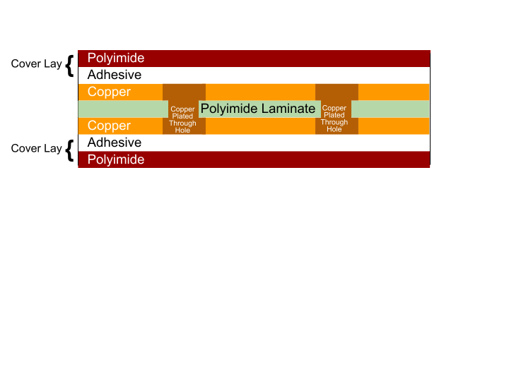
A double layer flex PCB
Multi-Layer Flex PCB
Multi-layer flexible circuits combine single and double-sided flexible circuitry designs. Inside, the middle section has dual-sided flex circuits, while the surface has a single-side conductive design covered in a protective film.
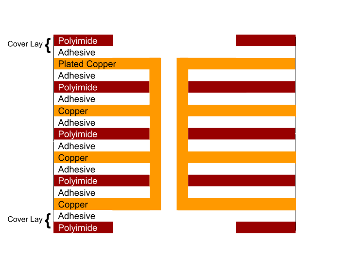
A multilayer flex PCB
Materials Used in Flex Circuits
| Layer | Material |
|---|---|
| Conductors |
|
| Adhesives |
|
| Insulators |
|
| Finishes |
|
Flexible PCB Design: How To Design Flex Circuits
| Step | Description |
|---|---|
|
|
|
|
|
|
|
|
|
|
|
|
|
|
|
|
|
|
Custom Flex PCB: Why Use Stiffeners in Flex Circuit Applications
Stiffeners improve the flex board’s reliability and durability, and they fall into three usage categories.
Rigidizing Connector and Component Stiffeners
These stiffeners create a rigid localized area suitable for mounting components or connectors.
They also protect the solder joints for these components from bending, which can damage the electrical link.

A PCB with a rigidized area for mounting a chip
ZIF Stiffeners
ZIF stiffeners create a thick, localized section at the ZIF’s fingers to meet its connection requirements.
Localized Bend Constraints
These stiffeners restrict bending at specific locations to meet the end application requirements, such as to allow final component assembly.
Factors Affecting the Cost and Turn-Around Time of Your Flex PCB
The primary factors affecting a flexible PCB's cost include the following.
- Materials
- Size and shape
- Number of layers
- Dimensional tolerance
- Board class or grade
- Via-hole features
- Drill hole size
- Copper foil thickness
- Circuit construction type
- Stiffener type
- Plating requirements
- Drill-to-copper distance
The manufacturing turn-around time is also important, and the factors that affect it include the following.
- Incomplete design data requirements
- Lacking information on the flexible-to-rigid transition zones
- Inappropriate bend requirements
- Missing ZIF connector specifications
- Other design-related issues
IPC Standards for Flexible Circuit Board Manufacturing
| No. | Serial Number | Name | Description |
|---|---|---|---|
| 1 | IPC-4203 | Cover and Bonding Material for Flexible PCBs | The standard classifies dielectric films (cover/base material) and adhesives, plus the qualification and quality requirements. |
| 2 | IPC-4204 | Flexible Metal-Clad Dielectrics for use in Flexible Circuit Board Fabrication | Metal-clad dielectrics are materials used in fabricating flexible PCBs. The standard classifies these materials and describes the quality requirements. |
| 3 | IPC-6013 | Performance and Qualification Specification for Rigid-Flex and Flexible PCBs | This standard specifies the qualification and performance for flexible circuit boards designed according to IPC-2221 and 2223. |
| 4 | IPC-FC-231C | Flexible Base Dielectrics for use in Flexible Printed Wiring | Revision C from April 1992 |
| 5 | IPC-FC-241 | Flexible Metal-Clad Dielectrics for use in Flexible Printed Wiring Fabrication | IPC-FC-241 describes the dielectrics for FPCBs and their quality requirements. |
| 6 | IPC-2223 | Flexible/Rigid-Flex Printed Board Sectional Design Standard | The standard highlights the requirements, interconnecting structures, and component mounting forms for flexible and rigid PCBs. |
| 7 | IPC-ML-990 | Performance Specification for Flexible Multilayer Wiring | 1972 Edition (September 1972) |
| 8 | IPC-FC-250A | Single and Double-Sided Flexible Printed Wiring Specification | This standard specifies the conductor patterns on the flexible base. They might have stiffeners or interfacial connections. |
| 9 | IPC-RF-245 | Rigid-Flex Printed Board Performance Specification | The 1987 Edition of IPC-RF-245, April 1987 |
How To Choose a Flex PCB Manufacturer
Flexible PCB manufacturers have increased over the years, but only a few meet the highest quality standards in manufacturing and storage.
You can determine the best by checking if they have quality, cutting-edge equipment for flex PCB manufacturing.
Also, ensure your manufacturer has trained, high-caliber technicians to handle the flexible circuit board fabrication process.
Ask if you can get a prototype made before going into full-scale production.
The manufacturer should be able to manufacture any flexible PCB you want for your project, whether single-layer, double-layer, multilayer, static, or dynamic.
Also, analyze the quality control measures they implement and check if they have the necessary accreditation and certification.
At a minimum, they should adhere to the industry’s manufacturing standards.
Remember to ask for a quote for a price comparison. Flexible PCB production shouldn’t be too costly, but an extremely low price is a reason to worry because price and quality go hand in hand.
Lastly, the manufacturer should provide proper storage or warehousing after manufacturing to keep the PCBs free from oxidation-related damage.
OurPCB: A Leading Flexible PCB Manufacturer
OurPCB is the top PCB manufacturer, and we have the expertise required to build any PCB type, including the flexible one.
We specialize in multi-layer flex and rigid-flex manufacturing and provide SMT component assembly for these boards.
We assure you of quality, reliability, and durability, meaning you can use our products in high-temperature, high-density applications worry-free.
Furthermore, our prices are reasonable, and we have a fast lead time of 5 - 6 days and 3 - 14 days for flexible and rigid-flex PCBs, respectively. The build time varies depending on the design.
Back to top: What is Flexible Printed Circuit Board (Flex PCB)?
Special Offer: Get $100 off your order!
Email [email protected] to get started!