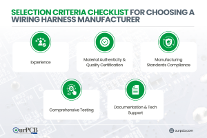
Top 10 Classic Car Wiring Harness Manufacturers | Full Guide
Finding the right wiring harness manufacturer for your vintage ride can be a real headache. Those beautiful old machines need special wiring that looks period-correct


Get high-quality PCB design services with OurPCB. We specialize in large-volume PCB fabrication tailored to your needs. Share your cost constraints and functional requirements, and we’ll handle the rest. With over 15 years of experience and satisfied customers worldwide, we ensure expertly designed PCBs. Request an online PCB quote today.


While you can use CAD software to draft designs yourself, professional PCB design services matter because they can help you ensure:
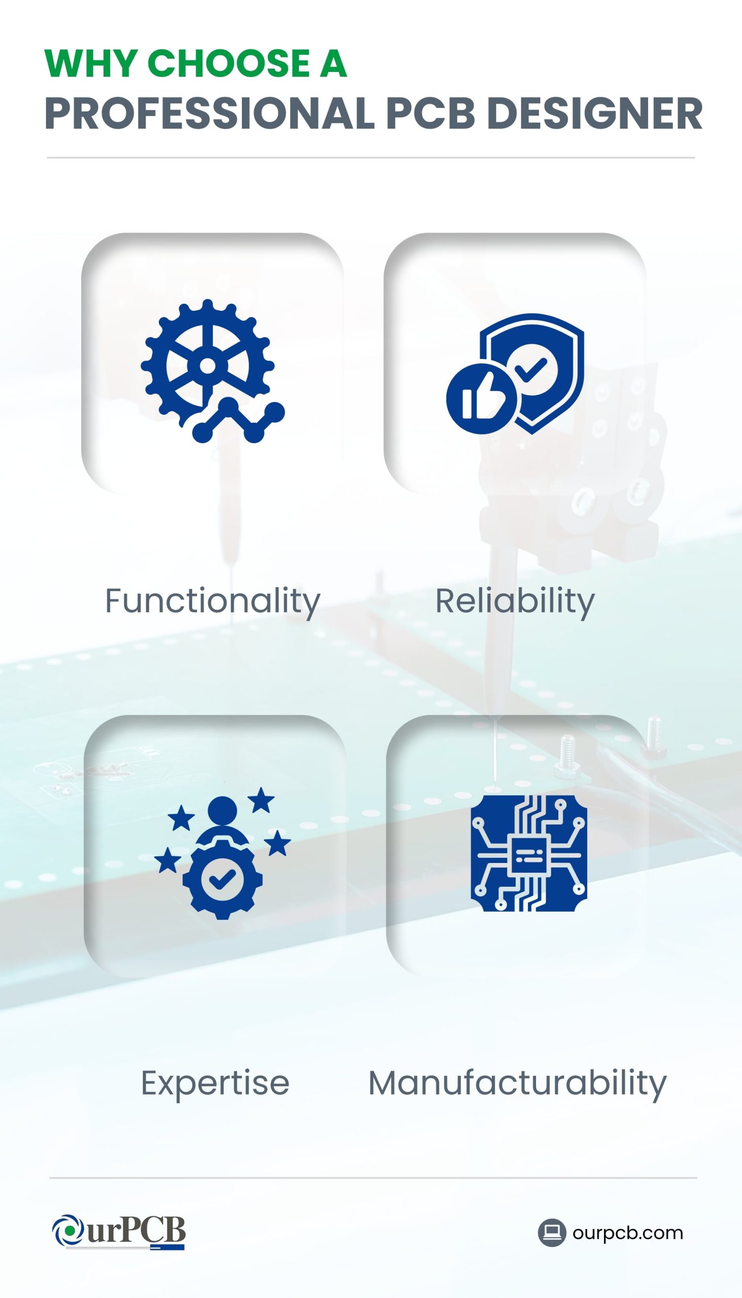

PCB design and fabrication service providers such as OurPCB can craft designs that are optimal for the manufacturing process. They can accurately translate schematics into fully functional boards.
Using professional PCB design services grants you access to experienced professionals. This minimizes the risk of errors, faults, and poor designs that are unlikely to perform well in the long run. Moreover, you can hold these professionals accountable if something goes wrong during the design or PCB manufacturing process.
Professional PCB Design services put you in touch with licensed professionals who understand the more specialized technical aspects of PCB design and fabrication. For instance, they can determine the best trace width and spacing to minimize electromagnetic interference (EMI). They can also organize components in a way that fully optimizes electromagnetic compatibility (EMC) and ensures strong signal integrity.
Professional design and fabrication service providers understand all requirements necessary to produce designs that meet manufacturing tolerances and specifications. By using OurPCB for your PCB design needs, you can reduce costs and the risk of reworks.
OurPCB is an industry leader in PCB fabrication and manufacturing that serves global customers. In addition to our modern fully-kitted-out factories in Shenzhen and Shijiazhuang, we have a branch in Melbourne, Australia that’s dedicated to serving our global English-speaking clientele.
In addition to our design services, we also troubleshoot and provide guidance on pre-established designs. We’ll help audit your schematics, guide you through the layout and routing process, and help you address and overcome any quick turn pcb boards assembly issues you may encounter.
The average hourly rate for PCB designs ranges from $95 to $145, depending on several factors. But this cost is not cast in stone as it depends on many conditions. These factors include the type of design software used, the number of component pins, the time required for the project, and the routing density of the PCB components. Get a FREE Quote Today
Our expert engineers craft precise and detailed schematic diagrams, no matter the complexity of your project.
Leveraging advanced tools such as Altium Designer, Cadence, Eagle, and KiCAD, we produce reliable and efficient PCB layouts tailored to your needs.
We provide end-to-end firmware development services to enhance the functionality of embedded systems seamlessly.
Custom software and app solutions according to your specifications.
We specialize in creating innovative algorithm solutions for a wide range of applications, including image processing and data analysis challenges.
Rapid prototyping and optimized designs with 3D printing and enclosure design expertise.
Mon-Fri: 24 hours,
Sat: 9am-6pm, GMT+8
Reach us at
[email protected]
24 hours online
+86-199-30589219
Mon-Fri: 24 hours,
Sat: 9am-6pm, GMT+8
Factors that influence the cost of PCB design include:
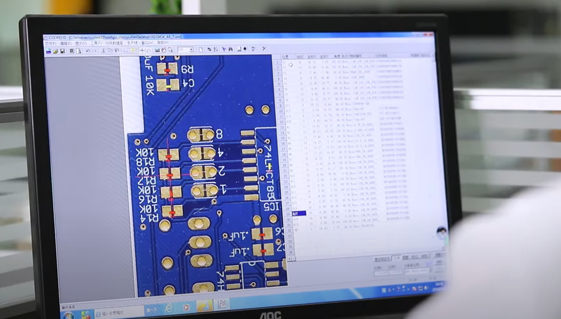
Design rule checks (DRC) are important because they ensure that PCB designs meet established standards and rules. For instance, the IPC-221A contains sections regarding density evaluations and placement requirements.
It’s good practice for technicians and designers to consult these sections when assessing designs. In addition to these rules, manufacturers may have certain constraints and restrictions that are unique to them. For instance, they may only be able to fabricate boards with a limited density or conformal coating thickness. Nevertheless, the main focus of DRCs is evaluating possible clearance, creepage, trace width, and via violations.
Performing a comprehensive DRC ensures that your designs are feasible for the fabrication process. As part of the DRC, designers and manufacturers may implement an electrical rule check (ERC). It evaluates the PCB’s electric design rules by verifying connections and scanning device information.
Finding the right wiring harness manufacturer for your vintage ride can be a real headache. Those beautiful old machines need special wiring that looks period-correct
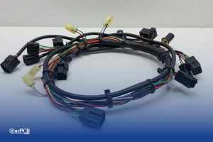
Would your car be able to run without wire harnesses? Not a chance. Wire harnesses connect all the electrical parts together. No harness means no
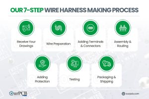
Making wire harnesses isn’t complicated. At OurPCB, we create custom wire harnesses for an expansive range of industries every day. While it’s a complicated process,

Prototype cable assemblies are the very important place in between PCB design ideas and interconnects. OurPCB brings prototype assemblies with PCB solutions to your tables.
PCB thermal management prevents component overheating through strategic heat transfer techniques. Without proper thermal control, electronics are at risk of electronic failures through weakened solder
ContentsKey TakeawaysWhat is a Multilayer-Printed Circuit Board?How do Multilayer PCB Boards Work?Multilayer PCB ApplicationsMultilayer PCB Manufacturing Process: StepsMultilayer PCB Manufacturing MachinesBenefits of Multilayer Circuit BoardsWhat
We use cookies to improve your browsing experience, which may include personal information. By clicking "Agree," you accept our Privacy Policy and cookie use. You can change your cookie settings in your browser anytime.
Agree
 Chat With Us
 Free Quote