Contents
- Key Functions of Surface Finish in PCB:
- Significance of Surface Finish in PCB Manufacturing
- Common Types of PCB Surface Finishes and Comparison
- 1. Hot Air Solder Leveling (HASL)
- 2. Lead-Free HASL
- 3. Organic Solderability Preservative (OSP)
- 4. Immersion Silver (Au)
- 5. Immersion Tin (Sn)
- 6. Electroless Nickel Immersion Gold (ENIG)
- 7. Electroless Nickel Electroless Palladium Immersion Gold (ENEPIG)
- 8. Electrolytic Wire Bondable Gold
- 9. Electrolytic Hard Gold
- How to Choose a PCB Surface Finish?
Key Functions of Surface Finish in PCB:
- Oxidation Prevention: Copper oxidizes quickly when exposed to air, making it difficult to solder. A surface finish protects the copper from oxidation, ensuring reliable solder joints
- Solderability: Different surface finishes provide varying levels of solderability. A good surface finish allows for easy soldering of components to the PCB
- Durability: The choice of surface finish can affect the durability of the PCB, especially in environments where the board may be exposed to moisture or corrosive elements
Special Offer: Get $100 off your order!
Email [email protected] to get started!
Significance of Surface Finish in PCB Manufacturing
The PCB surface finish impacts the following features.
- Process yield
- Inter-metallic joint quality
- Testing ability
- Manufacturing process cost
- Rework and scrap rate on the production batches
- Rate of board failure while being used for the intended application
Common Types of PCB Surface Finishes and Comparison
The following are the nine types of surface finishes.
1. Hot Air Solder Leveling (HASL)
Creating a HASL finish involves immersing printed circuit boards (PCBs) into a molten solder bath containing a tin/lead alloy. After that, you remove the excess solder and level the finish using air knives, hence the acronym HASL.
Besides, this leveling ensures a homogeneous solder surface finish thickness across the entire board. Also, the process helps identify potential delamination problems on the PCB before attaching costly components because it exposes the board to high temperatures. Moreover, HASL is mainly used on PCBs used for military applications.
Advantages
- Low cost
- Re-workable
- Long shelf life
- Widely available
- Excellent solderability
Disadvantages
- Creates uneven surfaces
- Solder bridging
- Contains Lead
- Not ideal for fine pitch pads and HDI structures
- High temperatures can affect other board materials
2. Lead-Free HASL
By comparison, lead-free HASL is similar to the traditional HASL but does not use the tin/lead solder alloy. Instead, it uses tin/nickel, tin/copper, or tin/copper/nickel/germanium alloys. Hence, the lack of Lead makes the process RoHS compliant and more economical. However, it is still not suitable for tiny components.
Advantages
- Low cost
- Lead-free
- RoHS compliant
Disadvantages
- First, it is not ideal for HDI applications
- Also, high processing temperature can affect other PCB materials
Finally, it can form tin whiskers
3. Organic Solderability Preservative (OSP)
OSP applies a thin, protective, water-based compound that selectively binds to copper pads. Moreover, this layer forms an organometallic surface that is more eco-friendly than other lead-free finishes because it is not toxic and consumes less energy. Additionally, the finish is becoming more popular due to its environmental friendliness, low maintenance, and suitability for fine-pitch applications.
Advantages
- Eco-friendly
- Re-workable
- Cost-effective
- Creates a flat surface
Disadvantages
- Impossible to measure the thickness
- Short shelf life
- Can cause IT issues
- Not ideal for plated through holes
4. Immersion Silver (Au)
Silver gets applied using an electroless immersion reaction, displacing the underlying copper layer. Immersion silver is not as reactive as tin, but it tarnishes when exposed to air. Therefore, you should store a PCB immersed in silver in anti-tarnishing packaging. It can stay for 6-12 months in this packaging. However, you must assemble the components via reflow soldering within a day once removed.
Advantages
- Ideal for fine pitch (tiny components)
- Excellent flat surface
- Re-workable
- Suitable for planarity
- Stable than other finishes
Disadvantages
- Sensitive to tarnishing and handling
- Requires special packaging
- Short operating window after unpacking
- Not ideal for micro vias with a 1:1 aspect ratio
- Unsuitable for peelable masks
5. Immersion Tin (Sn)
Immersion tin is a lead-free (RoHS-compliant) chemical process that is an excellent choice for tiny components and geometries.
It is the most cost-effective immersion coating type but has a few drawbacks. It tarnishes like immersion silver, giving you a 30-day window for soldering. Therefore, it will work well if you have a high production volume.
Advantages
- Excellent flatness
- Suitable for fine pitch (tiny SMD components)
- Good solderability after several thermal cycles
- Ideal for press-fit
- Mid-range cost
Disadvantages
- Sensitive to handling
- Short shelf life
- Not ideal to use peelable masks
- Can form tin whiskers
6. Electroless Nickel Immersion Gold (ENIG)
ENIG consists of a thin gold layer covering a nickel layer. The electroless nickel plating protects the exposed copper circuitry, while the layer of immersion gold protects the nickel during storage. Also, the layer of gold creates a low contact resistance.
This surface finish is arguably the most commonly used because it is tough and durable. However, it is expensive.
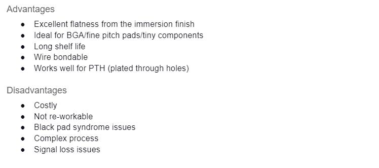
7. Electroless Nickel Electroless Palladium Immersion Gold (ENEPIG)
ENEPIG is relatively new because the technology hit the market in the late 90s. However, the 3-layer metallic coating was expensive and had few application demands.
But it made a comeback later due to its RoHS compliance, reliability, packaging needs, and suitability for high-frequency applications in compact spaces. Also, palladium prices have dropped significantly.
The process is similar to ENIG. But it adds an electroless palladium layer to stop nickel oxidation and prevent nickel corrosion & diffusion into the gold layer.
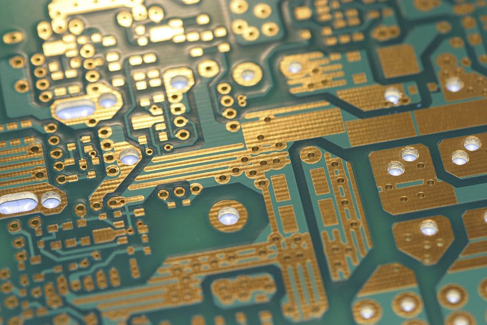
The gold-coated contacts on a PCB
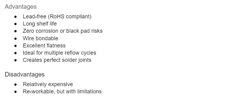
8. Electrolytic Wire Bondable Gold
Also known as soft bondable gold, this type contains a higher purity gold plating of 99.9%. Since the pad is usually a crowned surface, there's a smaller surface area to hold wires. Therefore, this finish is ideal for applications requiring wire bonding, high weldability, and high solderability.
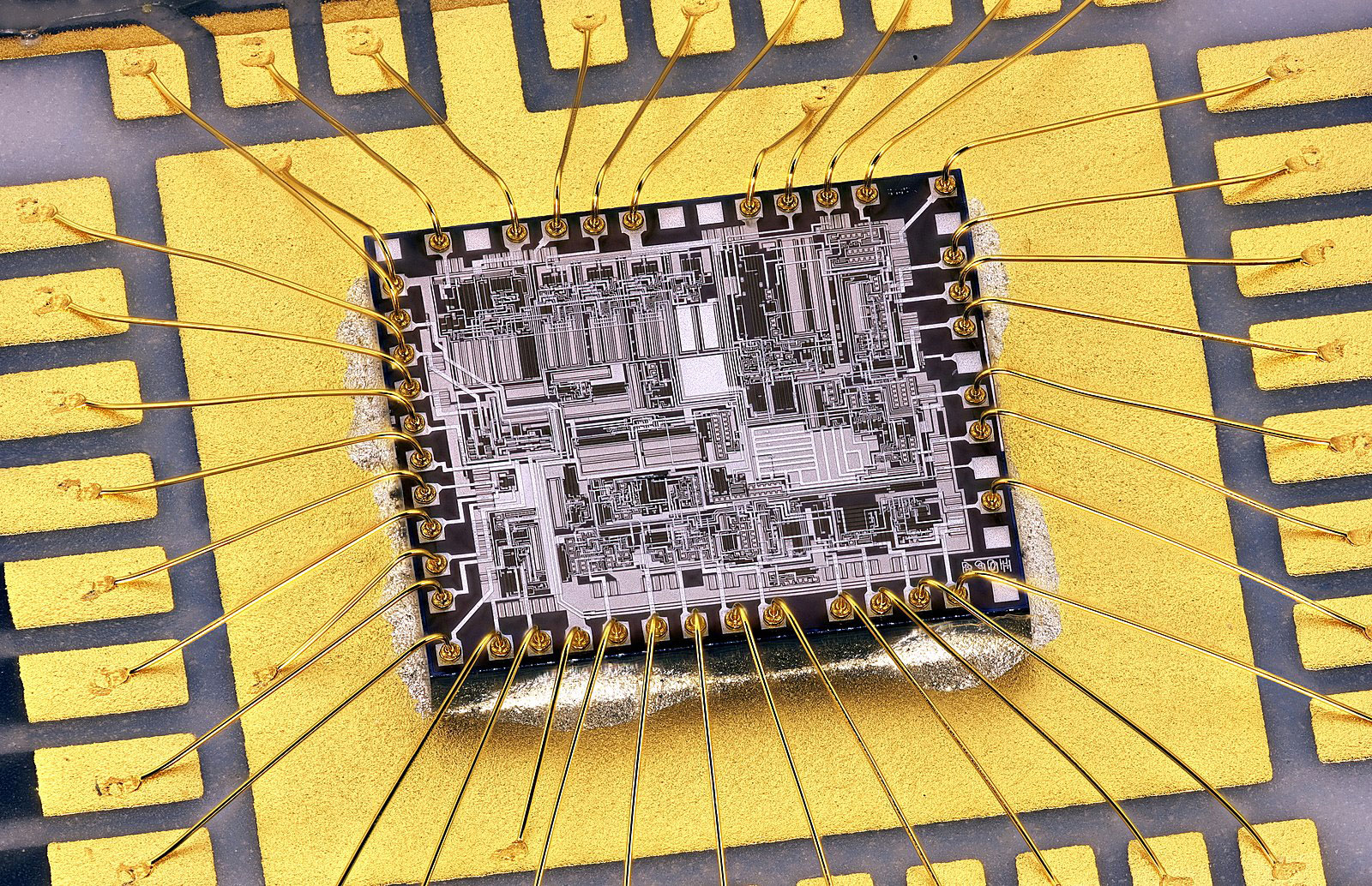
An IC mounted on a wire bondable gold PCB

9. Electrolytic Hard Gold
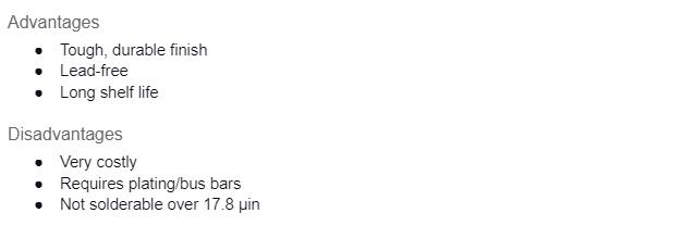
This finish consists of a gold layer plated over a nickel barrier coat. Hard gold is durable and typically used on keypads and gold fingers (edge connector-fingers). Also, you can control the gold thickness by varying the plating process duration.
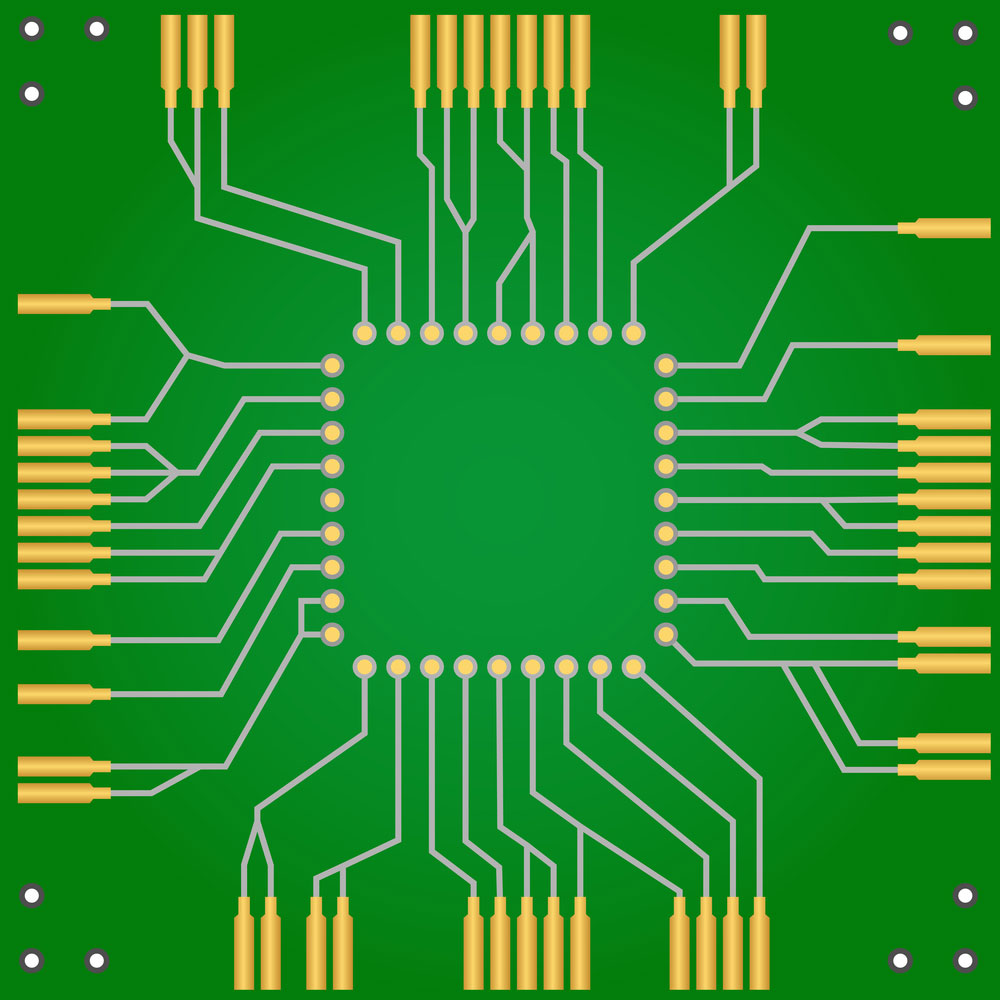
A green PCB with golden connectors
However, hard gold is not ideal for solderable areas due to its poor solderability and high cost.
How to Choose a PCB Surface Finish?
As shown above, the type of surface finish determines the durability and long-term reliability of the PCB. Therefore, you should consider the following factors when picking the best one.

For instance, HASL is best for military, space, and aerospace applications because it is highly reliable for high-performance applications. However, it is not ideal for aluminum wire bonding. Immersion tin and the organic surface finish in OSP are also unsuitable for aluminum wire bonding.
Ultimately, you need a knowledgeable and experienced PCB manufacturer to help you pick the best PCB surface finish for your project. OurPCB is the best in the industry because we have an extensive client list who continuously get high-quality products from us.
Special Offer: Get $100 off your order!
Email [email protected] to get started!


