As electronic devices advance, they use more powerful components and drivers that communicate through high-power, high-frequency signals. Traditional copper signal trace designs are not capable of handling this performance. However, you can design a controlled impedance PCB (printed circuit board) to take care of this.
With PCB-controlled impedance, you get several improvements, such as thicker and wider copper traces to transmit high-speed signals. At OurPCB, our manufacturing process places a focus on controlled impedance designs to ensure optimal performance for high-speed applications. If you're interested in our services, feel free to request a PCB assembly quote to learn more!
Contents
- What is Impedance?
- Components of Impedance
- Why is Impedance Control Important in PCBs?
- Maintain Signal Integrity
- Power Integrity
- Electromagnetic Compatibility (EMC)
- High-Speed Performance
- Applications That Require Impedance Control
- How to Achieve Impedance Controlled PCBs
- 1. Define Controlled Impedance Requirements
- 2. Select Appropriate Materials
- 3. Design the PCB Stackup
- 4. Calculate Trace Dimensions
- 5. Implement Design Rules
- 6. PCB Layout
- 7. Signal Integrity Analysis
- 8. Prepare for Manufacturing
- 9. Verification and Testing
- 10. Documentation and Iteration
- OurPCB: Controlled Impedance PCB Design
- FAQs on What is Impedance Control in PCB?
- What happens if I don't use controlled impedance in my high-speed PCB design?
- How does the dielectric constant of PCB materials affect impedance control?
What is Impedance?
Impedance is a measure of the total opposition that a circuit presents to alternating current (AC) when a voltage is applied. An impedance value is usually represented by the symbol Z and is measured in ohms (Ω). Moreover, impedance is an important concept in electrical engineering and electronics.
Specific impedance values can vary depending on the application and the specific requirements of a circuit. Here are a few common impedance values used in electronics and PCB impedance design:
- 50 Ω: Standard impedance value used in many high-frequency applications, including radio frequency (RF) circuits and test equipment
- 75 Ω: Used in video and cable television applications
- 100 Ω: Often used in differential impedance signaling applications, such as Ethernet and USB
- 300 Ω: Used in some antenna systems and older television applications
While these are the most common impedance values, the actual target impedance requirements can change depending on the impedance requirements of your circuit.
Components of Impedance
To understand impedance in a PCB design better, you’ll need to understand the components that impedance is made up of:
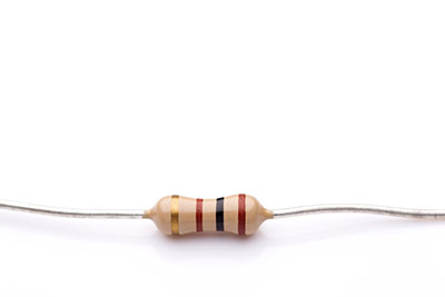
- Resistance (R): This is the opposition to the flow of electric current in a circuit. It's measured in ohms and is present in both AC and DC circuits. Resistance represents the real part of an impedance calculation, and it's always positive and constant for a specific material and temperature. It also causes power dissipation in the form of heat.
- Reactance (X): This is the opposition to changes in current or voltage due to inductance or capacitance. It's also measured in ohms, but it only exists in AC circuits. Reactance essentially represents the imaginary part of the impedance and can be either positive or negative. It doesn't dissipate power, but it does store and release energy, and is frequency-dependent.
Why is Impedance Control Important in PCBs?
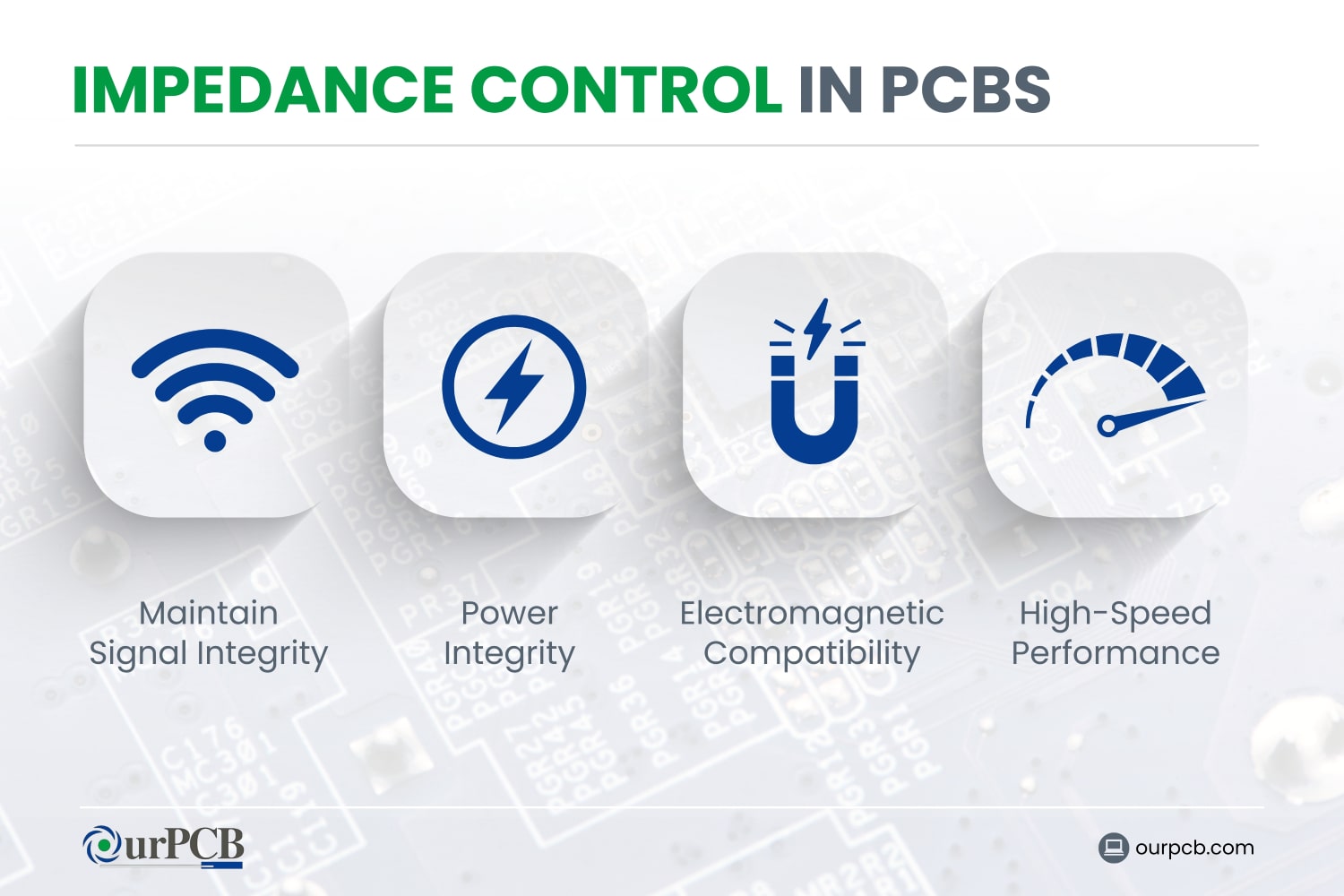
Let's get into why PCB impedance control is important. Essentially, it plays a major role in high-speed and high-frequency PCB designs. It improves the performance and reliability of electronic devices. Here are a few other reasons why impedance control is influential in PCBs.
Maintain Signal Integrity
With controlled signal integrity, you will have clean and reliable PCB signal traces and transmissions. A controlled impedance trace can minimize signal reflections and distortions and can maintain quality over a long PCB trace.
With a trace impedance mismatch, you may be faced with increased rise and fall times, ringing and overshoot, false logic circuit triggers, and more.
Power Integrity
Impedance control can help manage power distribution and reduce noise in power delivery systems. Essentially, maximum power is transferred only when the source impedance matches the load impedance.
In PCB assembly and design, a controlled PCB transmission line will ensure efficient power delivery to components and optimize signal strength in communication systems.
Electromagnetic Compatibility (EMC)
When you specify impedance control in PCBs, you can minimize electromagnetic interference (EMI) and improve the overall performance of your system. Impedance control is also important for meeting regulatory requirements, reducing interference with other devices, and improving overall system reliability, all of which contribute to maintaining optimal signal integrity.
High-Speed Performance
A PCB manufacturer will ensure impedance control because it's essential for high-speed digital circuits. It is also incredibly important for RF and microwave applications.
Special Offer: Get $100 off your order!
Email [email protected] to get started!
Applications That Require Impedance Control
There are several applications that require controlled impedance in PCB designs:
- High-speed digital applications like computer systems and networking equipment
- RF and microwave applications like wireless communications, radar systems, and aerospace and aviation equipment
- High-speed serial interfaces such as USB and HDMI
- Automotive electronics like Advanced Driver Assistance Systems (ADAS) and GPS navigation
- Industrial applications such as optical network equipment and 5G
- Internet of Things (IoT) appliances like smart home devices and wearable technology
In addition, PCB trace impedance control is critical for telecommunications, RF communications, high-speed computing, and consumer electronics. It is especially valuable for smartphones, tablets, and high-definition video equipment.
How to Achieve Impedance Controlled PCBs
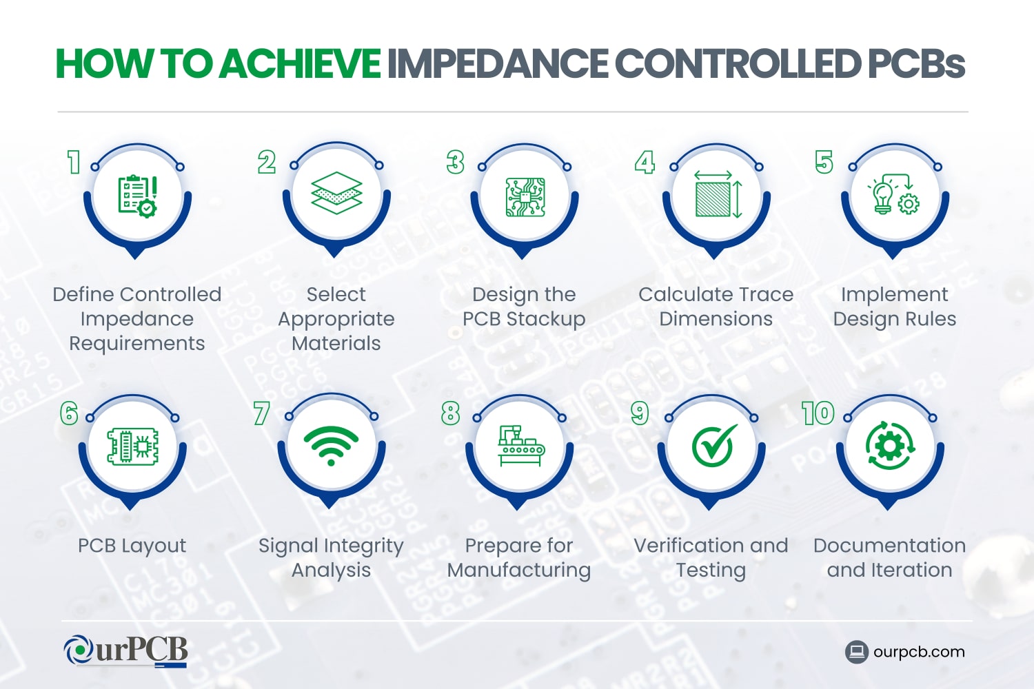

Achieving uniform controlled impedance in a PCB involves careful planning, design, and manufacturing considerations. Here's a step-by-step guide to help you understand how to achieve controlled impedance at each point.
1. Define Controlled Impedance Requirements
The first step is to define your impedance target. For single-ended traces on the PCB, the most common values are 50 Ω, 75 Ω, and 100 Ω. Differential pairs are 90 Ω, 100 Ω, and 120 Ω. Then, you're going to have to determine the frequency range of operation, as this affects the material selection and design rules.
Finally, specify your impedance tolerance limits. This is usually about 10%, but it can be tighter for more critical applications.
2. Select Appropriate Materials
It's important to choose the right PCB stackup. Select FR-4 for lower frequencies, but select high-frequency laminates for RF applications.
Lower dielectric constant (Dk) materials typically offer improved performance, while lower dissipation factor (Df) reduces signal loss. Then, be sure to choose the correct copper weight, often between 0.5 to 2 oz per square foot.
3. Design the PCB Stackup
Start by figuring out how many layers you'll need; more layers provide you with better control, but they also increase the cost. Arrange the signal and plane layers, typically as signal-ground-power-signal. Then, you'll calculate the dielectric thickness using impedance calculators or specialized software. For more complex designs, you might want to use buried and blind vias.
4. Calculate Trace Dimensions
Use impedance calculation formulas or software to calculate trace dimensions. You'll need to determine trace width and spacing and adjust these to calculate the impedance value. Also, keep in mind manufacturing tolerances. If you have differential pairs, you'll have to calculate the individual trace width and the spacing between traces.
5. Implement Design Rules

Set up the trace width and spacing rules in your CAD software and define size, spacing, and type via routes. Then you need to establish clearance rules for between traces, pads, and planes. Create length-matching rules for differential pairs.
6. PCB Layout
- Start by placing your components strategically, group related components, and minimize the trace length for critical signals.
- Route critical traces first to maintain consistent width and avoid sharp corners. Use your reference planes effectively to ensure a continuous return path and avoid splits under high-speed traces.
- Implement differential pair routing, keep traces close and parallel, and maintain equal length.
- After this, apply length-matching techniques and use serpentine routing when necessary.
- Finally, implement guard traces and stitching vias to reduce crosstalk and improve signal integrity.
7. Signal Integrity Analysis
Start by performing a pre-layout simulation using tools like HyperLynx or HFSS. Then, conduct a post-layout simulation to verify impedance control and make sure to check for reflections, crosstalk, and EMI issues.
Analyze eye diagrams to ensure that signal quality meets specifications and iterate design if necessary by adjusting trace widths, spacings, or stackup.
8. Prepare for Manufacturing
Generate accurate Gerber files and include impedance requirements in fabrication notes. Specify impedance control requirements, including target impedances for different trace types and acceptable tolerance ranges.
Then, request impedance coupons and test structures for impedance verification. Finally, choose a PCB manufacturer experienced in characteristic impedance control, like OurPCB.
9. Verification and Testing
Perform Time Domain Reflectometry (TDR) measurements to verify actual trace impedance. Use Vector Network Analyzer (VNA) for high-frequency testing to measure S-parameters. Then, conduct functional testing to ensure the PCB meets performance requirements. Analyze test results and make adjustments if necessary.
10. Documentation and Iteration
- Document all design decisions and test results
- Create a report detailing impedance control achievements
- Use insights gained to improve future designs
- Consider creating design guidelines for your organization
OurPCB: Controlled Impedance PCB Design
Controlled impedance PCBs are essential in modern electrical devices because they can handle high-power, high-frequency signals. OurPCB offers PCB manufacturing services that focus on controlled impedance designs, ensuring optimal performance for high-speed PCB Design applications.
By using thicker and wider copper traces, we help you achieve the necessary impedance matching for efficient signal transmission, enhancing the overall quality of your electronic devices. Get in touch to learn more!
FAQs on What is Impedance Control in PCB?
What happens if I don't use controlled impedance in my high-speed PCB design?
Without controlled impedance, you can experience unreliable operation, increased bit error rates, and in some cases, complete system failure. Particularly, you might see signal reflections, reduced signal integrity, EMI problems, power loss, and reduced maximum operating frequency.
How does the dielectric constant of PCB materials affect impedance control?
The dielectric constant affects the speed at which signals travel through the PCB. A lower Dk results in faster signal propagation and wider traces. The dielectric constant is an important part of calculating the impedance of a transmission line.
Back to Top: What is Impedance Control in PCB?
Special Offer: Get $100 off your order!
Email [email protected] to get started!


