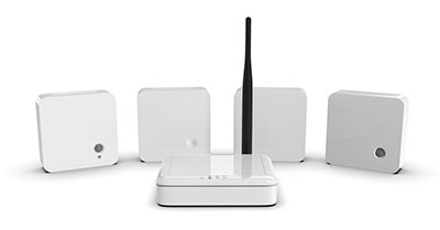
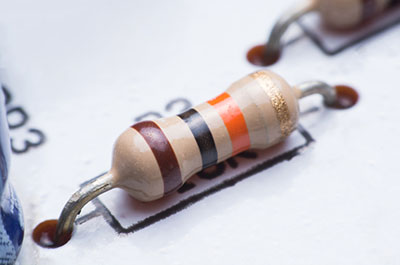
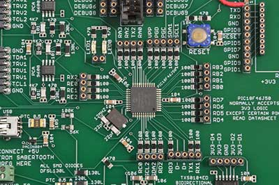
PCBs are critical in electronic devices and should have a long shelf life to maximize durability. One of the best ways to do this is by applying a protective surface finish to shield the copper layer. ENEPIG is one of the applied technologies in the printed circuit board fabrication process to create a protective finish that prevents copper oxidation. So, what is this technology, and how does it work? Let's find out.
Contents
- What is ENEPIG?
- How Does ENEPIG work?
- Copper Activation
- Electroless Nickel
- Electroless Palladium
- Immersion Gold
- ENEPIG vs. ENIPIG
- ENEPIG vs. ENIG
- Advantages and Disadvantages
- Application Comparison
- Technologies and Manufacturing Processes
- Considerations of Using ENEPIG Over ENIG
- Things To Be Wary About With ENEPIG?
- Cost
- Reliability
- Fractures
- Measures to Cost-Effective Surface Finish
- How To Solve the Black Pad Issue
- Summary
What is ENEPIG?
Nicknamed the universal surface finish, ENEPIG is an acronym for Electroless Nickel Electroless Palladium Immersion Gold. The metal plating gets its nickname from its ability to get deposited on almost any prototype PCB assembly.
ENEPIG has become popular in the recent past due to two reasons. It is highly effective in high-performance devices and has a low application cost compared to other gold plating types.
Gold is still expensive, but the price of palladium is significantly lower nowadays, making the technology more affordable than pure gold.
Moreover, the technology extends the shelf life of an ENEPIG coated board to well over one year, so you get good value for money.
How Does ENEPIG work?
To understand how ENEPIG works, we need to look at the four layers of metal structure that make up the finish. The process follows these steps:
Copper Activation
This process involves selectively activating the copper layer to determine the deposition pattern of the nickel layer in the electroless plating step. A displacement reaction creates a catalytic copper surface on which the nickel will sit.
Electroless Nickel
Copper can react with gold, so nickel is a barrier layer to separate the two metals. An oxidation-reduction reaction helps to deposit the nickel to the catalytic copper surface, creating a layer about 3 - 5 microns thick.
Electroless Palladium
The palladium layer acts as another barrier, but this time, it keeps the nickel from corroding and diffusing into the gold. Additionally, it acts as an anti-corrosion and anti-oxidation layer.
Like the electroless nickel application, this step involves using an electroless oxidation-reduction chemical reaction to make the nickel react with palladium. Depending on the application, the palladium layer can be 0.05 - 0.1 microns thick.
Immersion Gold
The last step is adding the gold layer to protect against oxidation and friction while giving low contact resistance. On top of that, gold helps to preserve palladium's solderability.
Immersion of gold involves fully immersing the PCB while using a displacement reaction to dissolve palladium and release electrons that reduce the surrounding gold atoms. The gold ions then attach to the PCB surface, replacing some of the palladium.
Thus, the result is a 0.03 - 0.05 thick micron gold plating layer, which is significantly thinner than other gold plating techniques.
ENEPIG vs. ENIPIG
The two acronyms almost resemble each other, but ENEPIG implements an electroless palladium process to apply the barrier layer. On the other hand, ENIPIG uses an immersion palladium process. Since the layering is the same, ENIPIG is also a universal finish.
However, immersion has a few weaknesses compared to electroless plating. It limits the thickness of the new layer and creates poor adhesion. Therefore, ENEPIG has the upper hand.
Special Offer: Get $100 off your order!
Email [email protected] to get started!
ENEPIG vs. ENIG
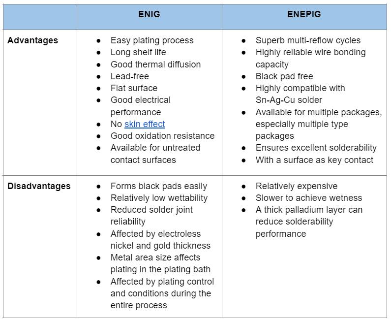
ENIG helped to do away with the disadvantages of OSP and HASL. These include flux elimination and flatness issues. ENEPIG came later as an improvement to ENIG by creating a thin palladium barrier layer to protect nickel from corrosion. By doing so, ENEPIG solves the common black pad problem in ENIG.
Also, ENEPIG has better wire bonding capability, a switch contact surface, and superb multi-reflow soldering capabilities.
These features enable it to meet stringent PCB requirements with multiple, high-density surface packages.
Both plating methods have their benefits and drawbacks, different applications, and manufacturing processes. Here is a close look at the two technologies.
Advantages and Disadvantages
Application Comparison
The advantages of the two technologies determine their most suitable application areas. ENIG is ideal for lead-free soldering, Ball Grid Array packages, Surface Mount Technology, and the like.
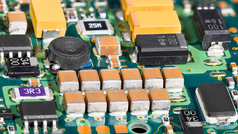
Surface Mount Technology
Considering the industrial applications, ENIG perfectly suits devices used in aerospace, military, telecom/data, and medical fields, as well as flexible circuits.
On the other hand, ENEPIG meets the more stringent requirements applied in Through-Hole Technology, BGA, SMT, press-fit, wire bonding, etc.
Therefore, you can use the technology in the aerospace and military industries and any high-performance devices requiring high component density and maximum reliability.
Technologies and Manufacturing Processes
ENIG's technology and manufacturing process involve three layers of metal structure: copper, nickel, and gold. Plating includes three functions: copper activation, Electroless Nickel Plating (ENP), and immersion gold.
However, ENEPIG takes four layers of metal structure. As described earlier, it adds a palladium layer and an extra electroless palladium process.
Considerations of Using ENEPIG Over ENIG
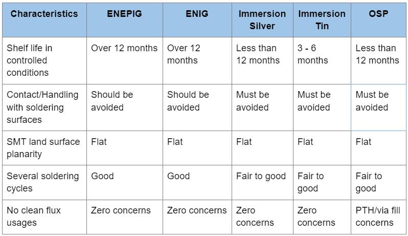
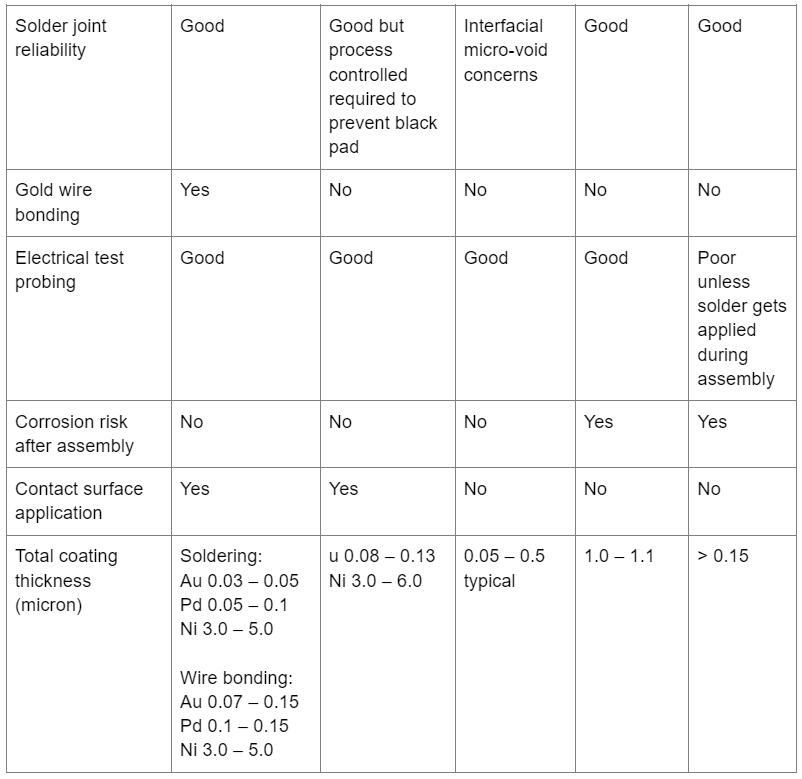
While ENIG is cheaper than ENEPIG due to the lack of the palladium layer, it is not as versatile as ENEPIG and cannot replace it in all applications. Here is a breakdown of why you should use ENEPIG over ENIG and other finishes.
Things To Be Wary About With ENEPIG?
Since ENEPIG plating is not a new technology, experts have studied its drawbacks extensively. Some of the things you need to look out for include:
Cost
Even though palladium prices have fallen drastically in recent years, gold costs remain high. Hence, the plating method is not that cheap. Additionally, the process tends to be wasteful if you don't need a gold wire bonding or lead-free coating.
Reliability
Due to the palladium distribution and copper presence, lead and tin bonding in ENEPIG might have some reliability issues. ENIG provides better bonding performance and reliability with these metals.
Fractures
The tin-palladium metallic layers form a brittle surface above the nickel plating, making it more prone to fracturing.
Measures to Cost-Effective Surface Finish
After going through the advantages and disadvantages of ENIG and ENEPIG, it makes more sense to pick the latter. However, its high price relative to ENIG puts it at a disadvantage.
The main issue with ENIG is black pad formation, so the plating method is viable if you solve this problem.
Since ENIG features an electroless gold layer, it is not possible to determine whether black pads exist or not.
Why? Nickel remains covered until the gold layer gets peeled off via a chemical method. Additionally, a P-rich nickel layer forms naturally after contact with nickel and gold and solder and nickel before and after soldering, respectively.
Therefore, the actual causes of black pads are:
- Poor technology implementation: Bad control allows crystal particles to form non-uniformly with many cracks.
- Long gold immersion period: Corrosion and cracks usually form on the nickel surface if this happens.
The solder mask also affects electroless nickel due to these reasons:
- The wrong solder mask leads to a degraded pad surface.
- Rigidity and insufficient cross bonding halt the copper activation reaction. In a hot electroless nickel solution, the solder mask monomer produces hydrogen, preventing the nickel reaction and breaking the chemical balance.
- Solder mask filled in the micro vias usually reacts electrochemically, stopping the creation of the catalytic copper surface in the process.
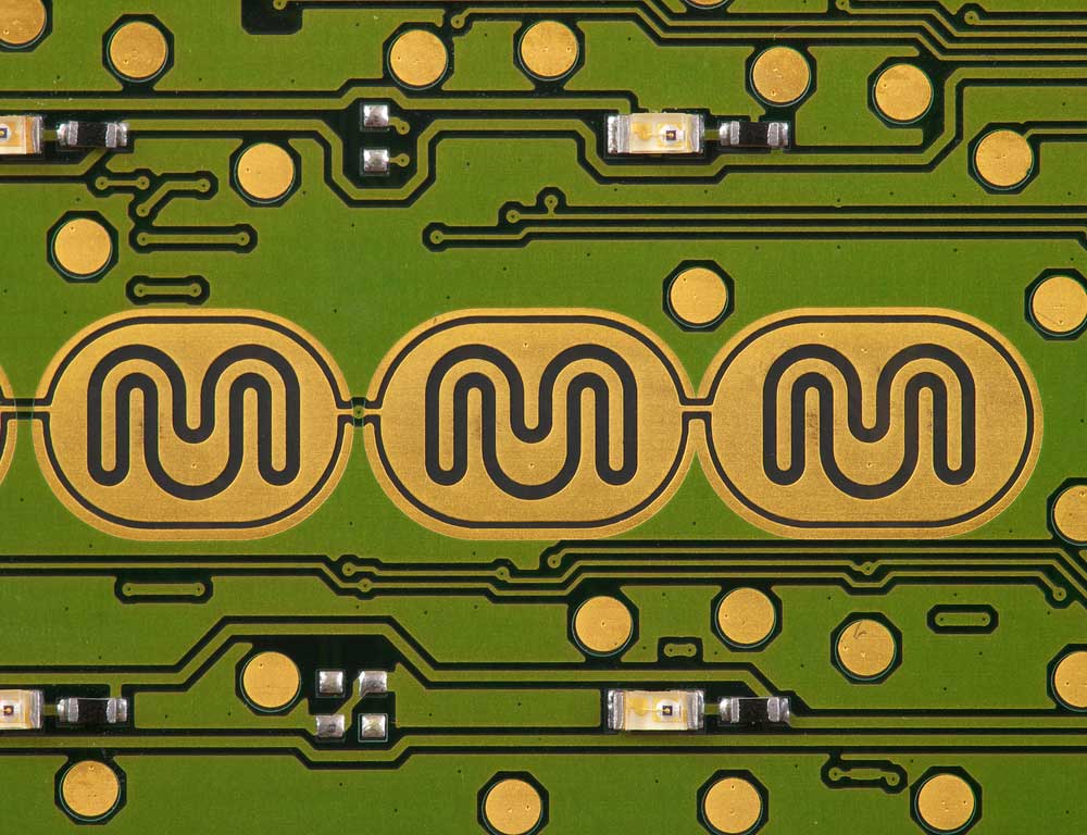
Gold-plated contact pads.
.
How To Solve the Black Pad Issue
Thus, to solve the black pad issue, the manufacturer must take these measures:
- Analyze the stabilizer content of the electroless nickel solution
- Control the pH value of the solution
- Stop nickel surface corrosion when immersing in gold
New immersion gold technology has proven effective in reducing plating costs while minimizing corrosion on the nickel surface.
It does so by:
- Creating a more neutral pH (7.0 - 7.2) to minimize corrosion
- Using a lower gold content to reduce the cost of raw materials and reduce the influence on the nickel surface
Also, the new technology produces nickel film with a columnar structure, so micro-cracks can only form on the surface.
Summary
Even though ENEPIG is not the cheapest PCB metal plating finish technology, it is one of the best to use on high-performance devices. As such, if you need an ENEPIG coat on your PCB for the demanding devices in your project, contact us today for more information.
Special Offer: Get $100 off your order!
Email [email protected] to get started!


