Printed circuit boards might seem easy to make, but the complexities of signal voltage transmissions and compact conductor spacing complicate their design. So you should understand concepts like differential pairs to make reliable high-speed circuit boards.
We will look at this concept in detail below to explain its advantages, disadvantages, and routing guidelines. Read on to learn more!
Contents
- The Basics of Differential Pairs in PCB Design
- Single-Ended Signaling
- Differential Signaling
- Advantages of Differential Signaling
- Zero Return Current
- Resists Incoming Crosstalk and EMI
- Resists Outgoing Crosstalk and EMI
- Low Voltage Operation
- Straightforward High/Low State
- Disadvantages of Differential Pair
- The Problems Associated with Diff Pairs in PCB Layout
- The Length of the Two Traces Must Be Equal
- Diff Pair Width and Spacing Must Be Consistent
- Differential Pair Routing Guidelines
- Route the Pairs Together
- Keep the Conductor Routing Symmetrical
- Keep the Length of the Conductor Pair Equal
- Conclusion
The Basics of Differential Pairs in PCB Design
Let's first understand the basics before we get into the advantages, technicalities, and difficulties of differential pair routing.
Single-Ended Signaling
Single-ended signaling is a simple, straightforward way of transmitting an electrical signal on a trace from a sender to a receiver and using a shared reference for the signal's return path.
The electrical signal is usually a varying voltage. It references the 0V node as the shared connection.
Most PCB nets use single-ended signaling routing, and you will need multiple conductors if transmitting several signals (one conductor per signal), plus a shared ground connection for all traces.
For instance, ten voltage signals require 11 conductors in total.
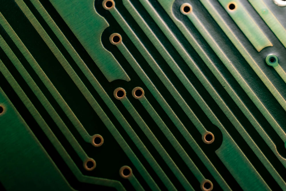
Conductive traces in a PCB
But there is a catch with this routing method. Issues like crosstalk and EMI can arise as transmission line speeds increase. So you might need differential signaling in such cases.
Differential Signaling
Differential pair lines use two complimentary voltage signal lines to transmit a single data signal, with the second signal line being the opposite of the first.
So a single information signal needs a pair of conductors, and the receiver deciphers the data by detecting the potential difference between the two conductors.
The signal voltages in the two conductors have an opposite polarity (relative to the common-mode voltage) and equal amplitude, making the return currents for these differential voltages balanced.
Therefore, differential pair signals have a net zero current flowing through the ground connection.
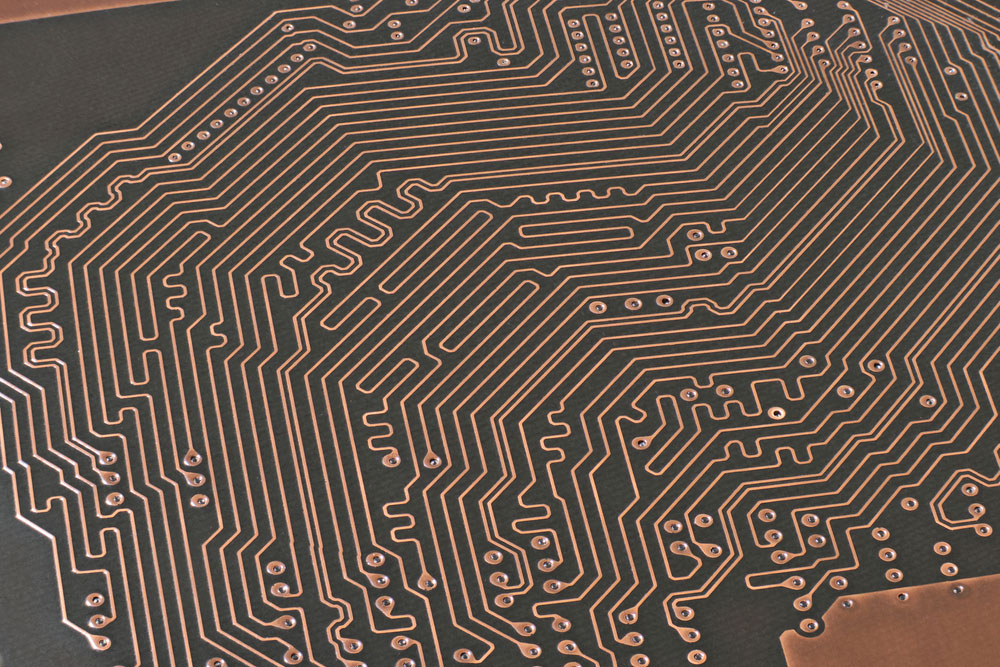
PCB traces with several pairs routed together
This setup brings about several benefits regarding crosstalk and electromagnetic interference reduction.
Also, differential signal pairs operate at lower power supply voltages. With single-ended signals, the traces must operate at higher voltages to ensure the signal-to-noise ratio (SNR) is sufficient for noise immunity.
An important thing to note with differential traces is the sender and receiver don't have to share the ground connection.
But potential differences in the ground planes will affect the circuit's operation.
Advantages of Differential Signaling
Although differential signal pairs need more conductors, they have the following benefits.
Zero Return Current
Since the differential pair lines balance out, they don't have a return current. Therefore, the ground plane is less relevant.
This plane can be different on the sender and receiver or fluctuate at a specific acceptable range.
But you must be careful when dealing with DC-coupled differential signaling, like USB interfaces.
These differential pair lines require a shared ground plane to keep the signals within the interface's minimum and maximum allowable common-mode signal voltage.
Resists Incoming Crosstalk and EMI
Electrical interference from nearby devices adds equally to the inverted and non-inverted signals.
So the pair is more resistant to common-mode noise because the receiver decodes the data by checking the potential difference between the two traces.
Additions to both signals will not change the potential difference, so the receiver's circuitry will reduce the noise amplitude to correct the voltage signal.

A signal on a TV screen with noise corruption
Resists Outgoing Crosstalk and EMI
Single-ended and differential signaling produces EMI when transmitting digital signals at high speeds (due to the rapid rising and falling edges).
But the electromagnetic interference generated in a differential pair will produce electromagnetic fields with equal magnitudes in opposite polarities.
So the noise will cancel each other out. This logic is the same behind the operational success of twisted pair ethernet cables.
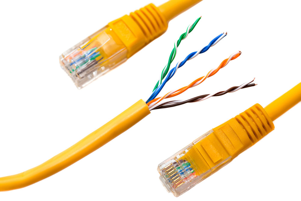
A twisted-pair ethernet cable
Low Voltage Operation
As stated earlier, single-ended traces must use a relatively high power supply voltage (3.3-5V) to maintain an adequate SNR for noise immunity.
However, differential pair signals can transmit signals at lower voltages while keeping the required SNR.
Plus, the SNR of these pairs doubles compared to equivalent single-ended systems due to the receiver's dynamic range.
Operating at low voltages implies a lower power consumption and tinier voltage transitions that help the board's power integrity.
Additionally, lower supply voltages radiate less electrical interference and allow you to use higher operating frequencies.
Straightforward High/Low State
With single-ended systems, receivers determine logic-high and logic-low states by checking the power supply voltage, the receiver circuitry's threshold characteristics, and the reference voltage value.
But tolerances and variations might bring uncertainties in determining the logic-high or logic-low.
Determining the logic states with differential signals is more straightforward.
The receiver interprets a logic high if the inverted voltage signal is lower than the non-inverted signal.
And the opposite results in a logic low.

A digital wave with logic highs (1) and logic lows (0)
Since the voltage has a continuous variation, it creates a transition point between the two states where the two signals intersect as they switch polarities.
This transition point is known as the crossover point.
For maximum timing precision, you should match the conductor length for the differential pair.
If unequal, there will be differences in signal propagation, causing delays that shift the crossover point. In such a case, this point will not match the logic transition.
Special Offer: Get $100 off your order!
Email [email protected] to get started!
Disadvantages of Differential Pair
This routing method has a few disadvantages, the most obvious being an increase in the number of conductors.
For instance, you'll need 21 conductors to handle only ten signals. These will take up lots of space on the board.
Other issues include the following.
- Needs careful routing considerations (space, length, & impedance) and procedures
- The circuit can have noise signals if routed incorrectly
The Problems Associated with Diff Pairs in PCB Layout
Besides using two conductors per signal, designers must contend with the following issues when laying out differential pairs.
The Length of the Two Traces Must Be Equal
One of the best benefits of differential signaling is that it cancels out incoming & outgoing noise because the two conductors create some equilibrium.
However, you will not achieve this balance if the lines don't have the same length, which will allow common-mode noise interference and other EMI issues.
These problems worsen the more the signals have higher rise and fall times.
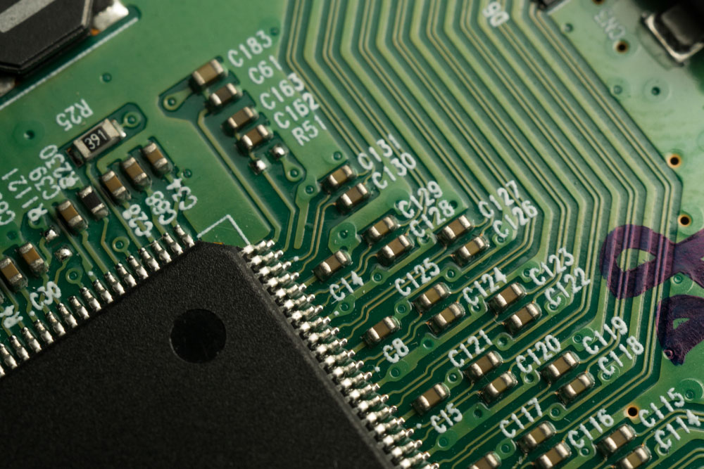
Differential signal lines for an IC mounted on a PCB.
Diff Pair Width and Spacing Must Be Consistent
Differential impedances resulting in mismatches and noise/EMI introduction can arise if the traces are far apart and have different widths.
So you should route them together and ensure they have the same width even when circumventing obstacles like components and vias.
Differential Pair Routing Guidelines
Adhere to these guidelines to get stable and reliable differential pair signals.
Route the Pairs Together
Besides identifying the conductors clearly for routing as pairs, avoid using vias to keep the spacing between them consistent.
And if you must use vias, use them as symmetrical pairs and position them close to each other. Also, place the vias at an equal distance from their pads.
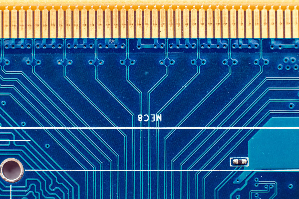
Differential pairs with symmetrical vias
While at it, prioritize inner layer routing to reduce crosstalk. However, internal layer routing means using vias to connect between different layers.
And remember to isolate the diff pairs from other traces by specifying a clearance of 3W, where W is the regular trace width spacing.
You might have to consider broadside differential pair routing on the adjacent signal layers to allow for more efficient crosstalk control and higher routing densities.
Keep the Conductor Routing Symmetrical
Ideally, the conductors in diff pairs should mirror each other, and you can use these tips to make that happen.
- Plan the routing to maintain symmetry by avoiding components and vias
- Maintain consistent spacing between the pair
- Plan your pad's route for entry and exit to enable conductor mirroring
- Maintain the same trace width across the conductor's length
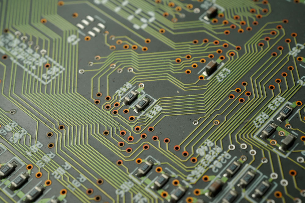
Signal traces on a PCB.
Keep the Length of the Conductor Pair Equal
Lastly, you have to route the conductors to have the same length. You might have to insert tiny trace-tuning sections on the shorter transmission line to make it longer and match its twin.
This addition might alter the pair's symmetry, but length equality is more important. If the inequality occurs due to non-symmetrical pad locations, insert the trace tuning in that area.
Conclusion
As you can see, differential pairs introduce benefits, like common-mode noise immunity and low voltage operation, which are critical for high-speed signal transmission in circuit boards.
Although you need double the number of conductors to handle one signal, the routing method is essential for modern high-speed circuits.
Laying out the conductor pair route might be challenging, but you can achieve it using the guidelines above.
And contact us if you encounter any challenges in the design process. We'll be happy to help.
Special Offer: Get $100 off your order!
Email [email protected] to get started!


