Generally, we use switch-mode supplies in many electronic processes such as DC to DC converters. However, there are times when the available battery voltage of a DC supply may be insufficient to operate the system. And even if you use more battery banks, you'll' only end up adding bulkiness and taking up more space. A quick solution to this challenge is to boost the available DC voltage and use fewer batteries in the process. And that's how to boost converters comes in handy.
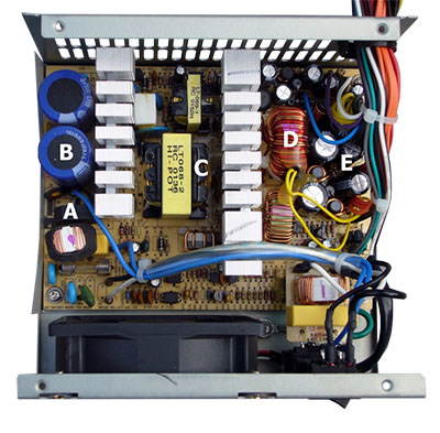
(interior of a switch-mode power supply device)
Contents
1. What is a Boost Converter?
A boost converter is a type/form of switch-mode converter that increases or boosts an input voltage. Often, it comprises components such as a diode, capacitors, MOSFET or semiconductor switch, and an inductor. Therefore, when compared to sole inductors or AC transformers, a boost converter is less bulky.
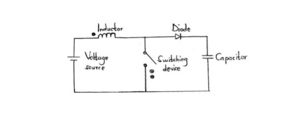
Boost converter circuit diagram
A boost converter may need a periodic square wave source that can either be an SMPS IC or a 555 timer to function. What's more, its working efficiency sometimes reaches a 99% level of functioning.
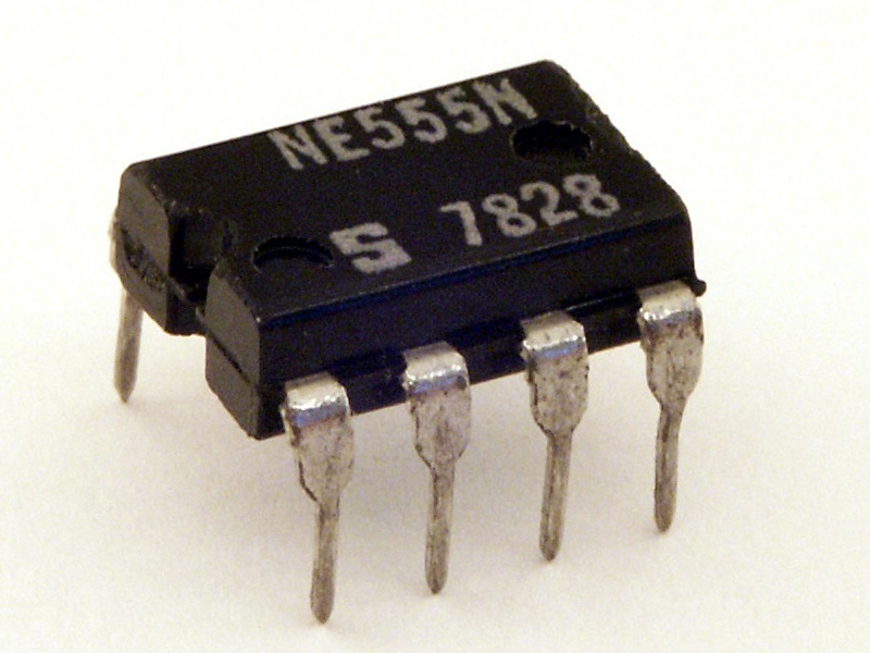
(555 timer IC)
Then, it's mandatory to differentiate between a buck-boost converter, a buck converter, and a boost converter.
Buck-boost converter; Here, a buck and boost portion work in coordination to regulate voltage in applications such as power supplies, power amplifiers, and consumer electronics.
Practically, the boost part will make the input voltage generate a greater output voltage to charge up a device.
Then, the buck part will recognize the almost fully charged system and gradually lower the voltage to prevent overheating. After getting to the maximum charge, the system's voltage will drop to zero.
- Buck converter; It steps down the voltage from its input to output voltage while stepping up the input current. A boost converter works oppositely. That is to say; it steps up the input voltage then steps down the input current.
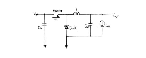
Circuit of a buck converter
Special Offer: Get $100 off your order!
Email [email protected] to get started!
2. How Does a Boost Converter Work?
Before we focus on how a boost converter works, you should revisit the working principles of diodes, inductors, capacitors, and MOSFETs. Diodes and transistors are active semiconductors, while a capacitor or inductor can be a passive component.
So, how does a boost converter work?
- The first step begins with a level of inactivity. The circuit has the output capacitor charging into the input voltage with less than one diode drop.
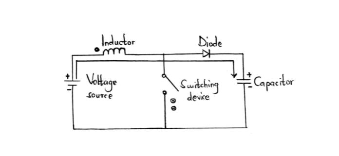
Step 1 circuit diagram on boost converter working.
-
For the second step, you should switch ON the circuit.
Immediately after switching, the signal source becomes high, then turns on the MOSFET. Consequently, there's a current diversion to the MOSFET via the inductor.
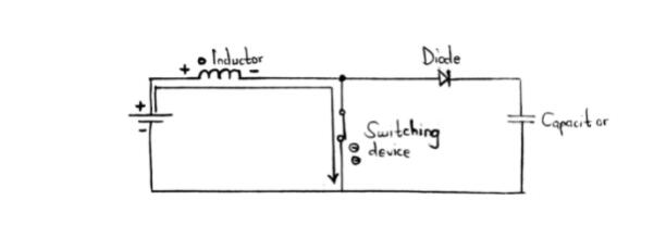
Step 2
Note; Since there's a back-biased diode state, you should ensure the output current remains charged. Also, you can get the converter's DC input from various sources and batteries like DC from solar panels, DC generators, rectified AC from a mains supply, and fuel cells.
The power source doesn't' get an immediate short circuit because the inductor provides a gradual ramping up of the current. Then again, there's a buildup of a magnetic field around the inductor.
- In the third and final step, a MOSFET turn-off also halts the current to the inductor. Inductors like to maintain a smooth current flow. In this case, however, the abrupt electric present change causes it to produce a large voltage. The voltage has an opposite polarity to the original voltage supply. Then, it maintains the large current flow using the surrounding magnetic field.
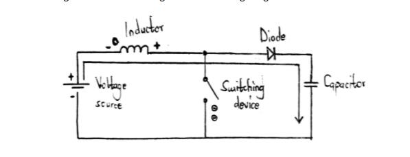
Step 3 on Boost converter working.
In the end, when we are keen on the polarity symbols, we see that the inductor behaves like a voltage source. And, it is in series with the supply voltage. In other words, the diode's anode has a higher voltage compared to the cathode. Additionally, it is forward-biased.
Further, the charge to the output capacitor is of a higher voltage than formerly, which symbolizes an upgrade from a low DC voltage.
3. Boost Converter Modes of Operation
You can operate the boost converter in two different operation mode systems.
-
The continuous mode
For the mode here, when the transistor is switched off, the inductor current won't get to zero while in the discharging process. It often happens when a dimensioned transistor has an inductor that always connects back quickly with the input supply via a switched-on transistor. The connection occurs before a current discharge across capacitor C and the load. As a result, the inductor has a consistent and effective rate of boost voltage production.
-
The discontinuous mode
On the contrary, the transistor here can have a wide switch ON timing. And so, the inductor can discharge fully and maintain inactivity during the transistor's button ON periods. In that way, a large current ripple voltage comes about across the capacitor C and load, leading to fluctuations and less efficient output.
Generally, we can calculate the best yielding maximum stable voltage of ON/OFF times by ensuring the inductor has an optimal switching. In that way, neither a late switch ON can drain the voltage inefficiently nor a too quick button ON that can discharge current optimally.
4. How to Design a Boost Converter
For an outstanding boost converter design, use the steps below;
Step 1
Start by determining the output current and output voltage separately. It helps us ensure we have the correct, current load and also generates substantial output power.
Step 2
Secondly, we will divide the output power by the input voltage to get a recommendable average input current. To account for situations like ripples, increase the rate of the input current by 40%. Then, label the value you have after this as the peak input current.
Under any circumstance, the minimum input current is always 0.8 times the stipulated average input current. Therefore, you should multiply the average input current you got by 0.8.
Finally, we have two values, the minimum and peak current. If you wish to get the total change in current, subtract the minimum from the peak current.
Step 3
The third stage involves a calculation of the converter's duty cycle. A duty cycle refers to the off and on times of an oscillator.
For that, use the formula provided below;
D.C. = (Vout – Vin) / (Vout)
The resulting decimal value should be below 0.999 and above 0.
Step 4
The next step involves finding the frequency value of the oscillator. Since the signal source varies, i.e., can be from a fixed frequency PWM controller or a 555 timer, we will make this a separate step. In a case where you'll use a 555 timer, you'll' completely control the duty cycle and frequency.
After getting the frequency, we will take its inverse as the total period. Then, multiply the duty cycle and period to get the value of on-time.
Step 5
Last but not least, now we have the values of change in current, on-time, and input voltage. When we introduce the three into an inductor formula, it should be as follows;
L = (V*dt) / dI
Whereby;
V = input voltage,
dt = on-time, and
dI = change in current.
If your resulting inductor value isn't' usually accessible, you can switch to a closely available value. Just tweak it a little, and the system will be good to go.
Parts list for the Boost Converter
-
Output diode
Depending on the type of converter you want, you should settle for a worthwhile output diode. For example, you can use a Schottky diode such as a 1N5822 to build a low voltage converter (between 3.3V and 5V).
-
Switching transistor
As for the switching transistor, one with a higher breakdown voltage than the converter's maximum output voltage is ideal. Often, you can achieve this by going through the MOSFET's datasheet and ensuring your choice has a low input capacitance/gate capacitance. Common values equate to easy driver requirements.
Moreover, using a MOSFET gate driver is highly recommendable because it saves on time and losses.
Conclusion
To sum it up, the boost converter technology still contributes to a regulated low voltage DC or DC power supply throughout modern electronics applications such as mobile phones. Now that we have spilled some knowledge on how you can build your boost converter and its working principle, you may go on ahead and surprise your tech skills.
And if you get stuck in the process, don't' hesitate to reach out to us. Our electrical engineering professionals are always at your service.
Special Offer: Get $100 off your order!
Email [email protected] to get started!


