China HDI PCB Board

iso
ISO 9001/UL Certified
icon assembly
PCB Assembly Specialists
icon truck
97% of PCB Shipped on Time
icon time
98% of PCB Delivered to Spec
icon guarantee
Delivery Guarantee

China HDI PCB Manufacturers

PCB Manufacturing Process

online quote
Online Quote
upload pcb
Upload PCB File
order review
Order Review
payment
Payment
order update
Order Updates
truck
Delivery
confirm
Confirm Received

The Benefits of Partnering With OurPCB for China HDI PCB Boards

sp3
moon shape
wave w
Advanced Technology
  • Latest laser drilling and imaging systems
  • Precision sequential lamination processes
Quality Assurance
  • Rigorous testing at each production stage
  • IPC Class 3 standards compliance
Competitive Pricing
  • Efficient production lowers costs
  • Bulk order discounts are available
Responsive Support
  • 24/7 customer service
  • Quick quote and design feedback

Why Choose a China HDI Circuit Board?

Space Savings
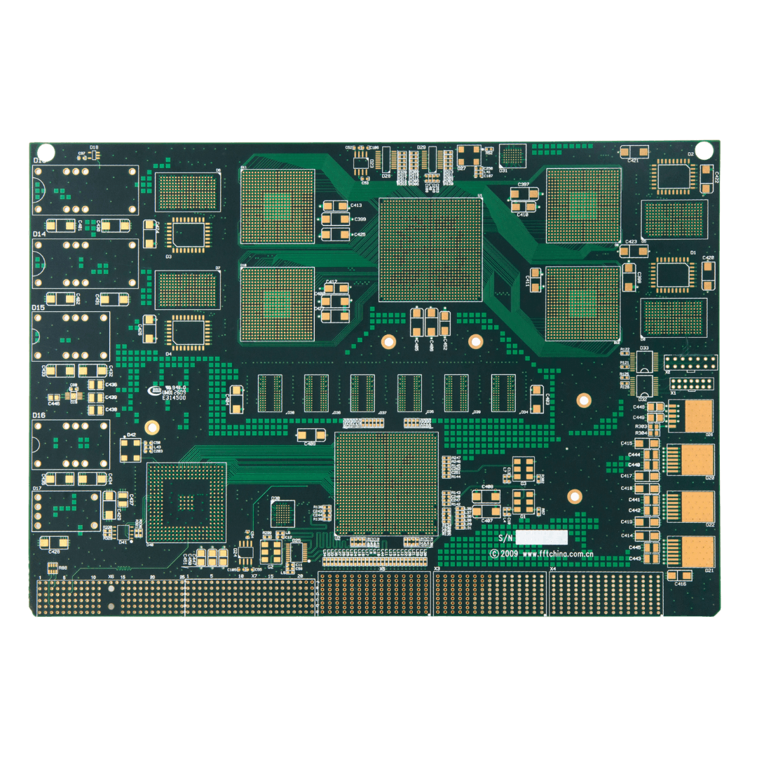
  • Smaller board sizes are possible
  • More components in less area
Improved Signal Integrity
  • Shorter signal paths
  • Less electromagnetic interference
Higher Circuit Density
  • More traces per layer
  • Increased functionality in the same space
Cost-Effective Production
  • Lower material costs at scale
  • Efficient manufacturing processes
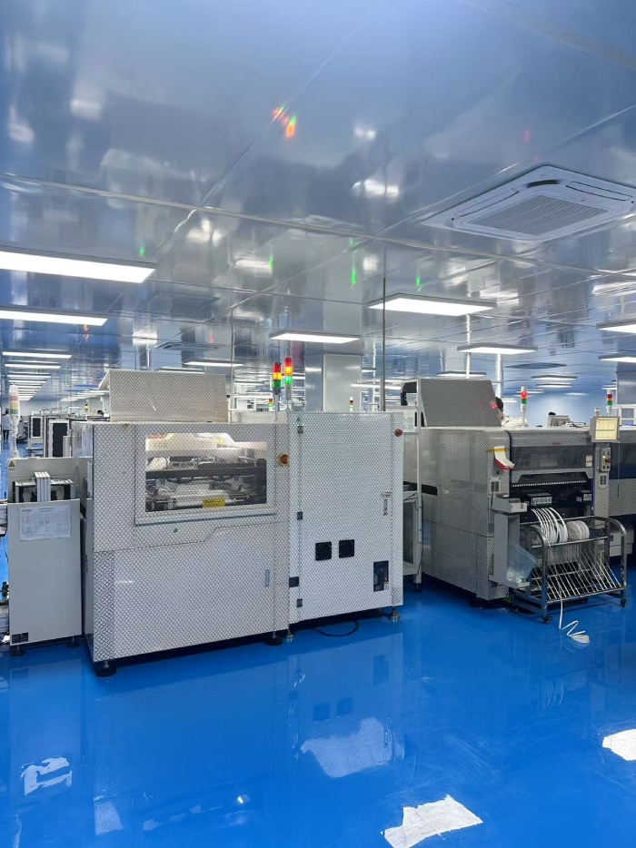
sp1
sp2
sp3
sp3
moon shape
wave w

PCB Assembly Services

OurPCB provides full PCB assembly services. We can handle all aspects of bringing your China HDI PCB design to life.

Millions of business and innovators use OurPCB

PCB Board Process

Design (1 day)

  • Upload Schematic to Get a Quote
  • PCB Review and Quotation
  • Customer Makes Payment
  • Evaluation & Confirmation of Plan
  • Design Start

Layout (1 day)

  • Layer Stack-up Design
  • Design Rule Setting
  • Component Placement Design
  • Confirmation & Optimization
  • Fanout

Routing (1 day)

  • Fanout Optimization
  • PCB Routing
  • Equal-length Adjustment
  • Routing Optimization
  • DRC Check
  • Routing Confirmation

Optimization (1 day)

  • Silkscreen Adjustment
  • Data Output
  • Customer Final Confirmation
  • Production Debugging
  • Archiving Projects
  • Finish

PCB Board Process

Order Received

  • Component Procurement
  • Preparation
  • PCB Manufacture
  • Make Process Flow

Soldering

  • Solder Printing/Wave Soldering
  • SMT/Plugging
  • Inspection (repair if necessary)
  • AOI (repair if necessary)
  • Transfer

Parts Assembly

  • Manual Assembly
  • PCBCleaning
  • Wire Screw
  • Inspection
  • Repair If Necessary

Finalization

  • Final Confirmation
  • Packing
  • Shipping

Technical Capabilities

wave w
mcd
sp3

Capabilities & Services

FAQ's

What is HDI in PCBs?

HDI printed circuit board technology enables high-density interconnection for miniaturized electronics. It uses blind and buried vias to increase routing density effectively. The layers of a PCB in HDI designs are tightly packed. HDI PCB production enhances electrical performance and reduces signal loss significantly.

What is the difference between HDI and non-HDI PCB?

High-density interconnect PCBs have more complex layer structures than standard boards. The layer of the PCB in HDI designs supports finer traces and spaces. Non-HDI PCBs lack blind and buried vias for enhanced connectivity. HDI PCB made in China is widely used for advanced applications.

Are there any design guidelines for HDI PCBs I should follow?

Ensure proper HDI PCB stackup service to optimize electrical and mechanical properties. Choose a reliable China HDI PCB factory for consistent quality and precision. Leading China HDI PCB board manufacturers offer tailored solutions for complex designs. A trusted PCB supplier helps streamline PCB production for improved efficiency.