


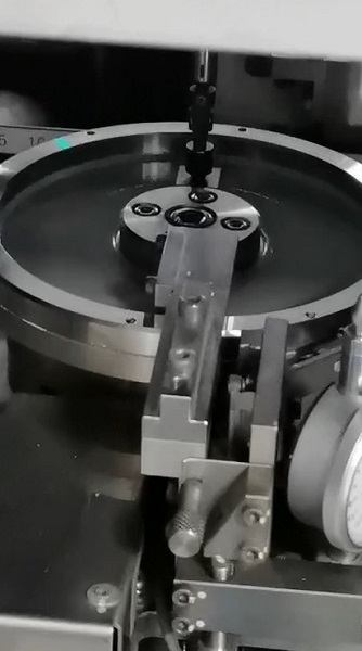
- State-of-the-art equipment for precise package alignment
- Advanced reflow systems for reliable solder connections

- Rigorous inspection processes at every stage
- Adherence to industry standards for reliability

- Support for various package types and sizes
- Custom solutions to meet specific project requirements


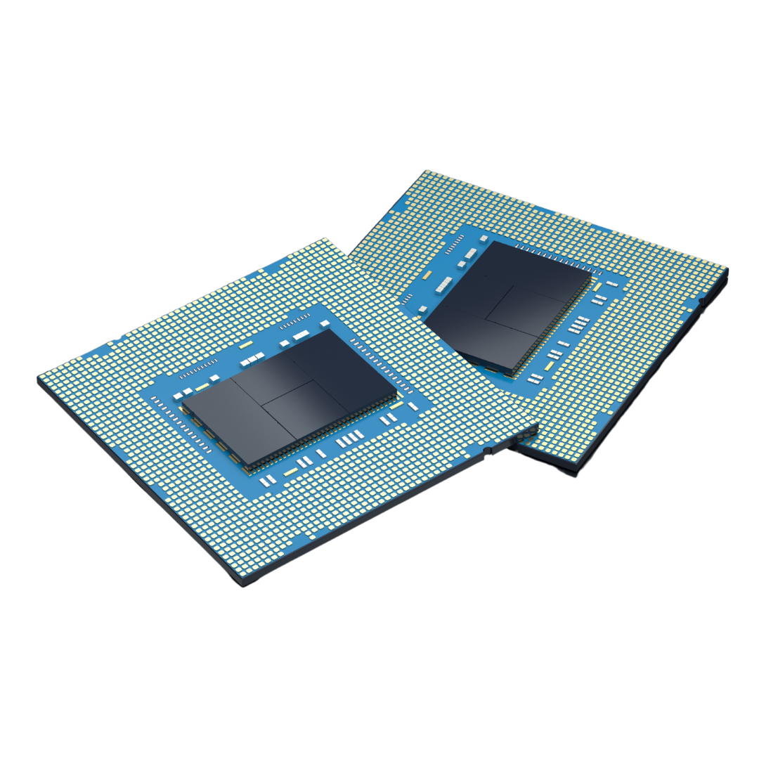
- Integration of multiple chip functions in a single package
- Improved signal integrity between logic and memory

- Vertical stacking reduces PCB footprint
- Allows for smaller, more compact device designs

- Shorter interconnects between chips
- Reduced signal delays and power consumption

- Mix-and-match capability for different chip combinations
- Easier upgrades and modifications of memory components

- Integration of multiple chip functions in a single package
- Improved signal integrity between logic and memory
- Vertical stacking reduces PCB footprint
- Allows for smaller, more compact device designs
- Shorter interconnects between chips
- Reduced signal delays and power consumption
- Mix-and-match capability for different chip combinations
- Easier upgrades and modifications of memory components

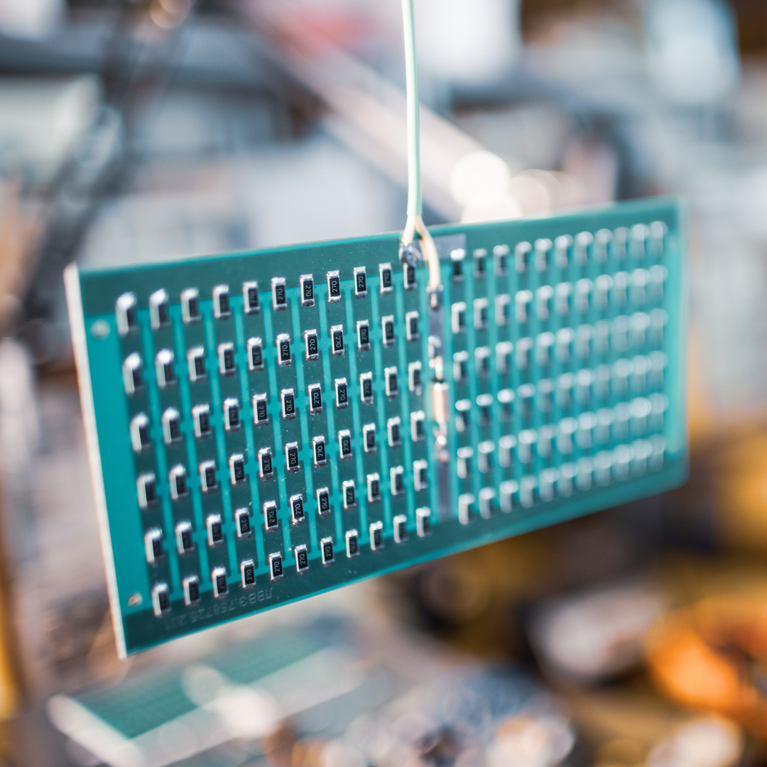
We use advanced Surface Mount Technology for high-density, compact PCB assemblies. Our SMT process ensures precise component placement and reliable connections.

We adapt to your needs, working with your supplied components or providing full turnkey solutions. Our services cover everything from sourcing to final assembly.

Our team creates tailored PCB assemblies to match your exact specifications. We handle unique designs and special requirements with skill and attention to detail.

We offer fast, high-quality PCB assembly services. Our efficient processes deliver quick turnarounds without compromising on quality or reliability.

We produce PCB assemblies that meet strict IPC Class 3 standards. This ensures top performance in critical applications like aerospace and medical devices.

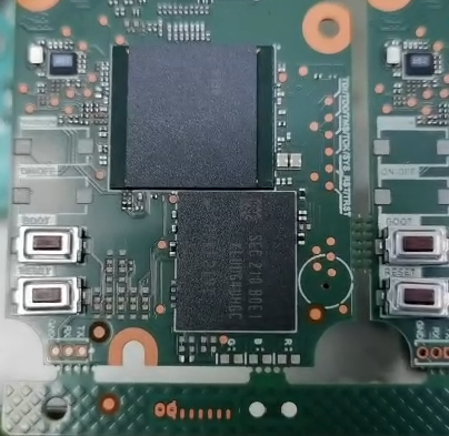
We handle a wide range of IC package types in our PCB assemblies. This includes BGAs, POPs, CGAs, QFNs, DFNs, and CSPs, all assembled with precision.
Mon-Fri: 24 hours,
Sat: 9am-6pm, GMT+8
Reach us at
[email protected]
24 hours online
+86-199-30589219
Mon-Fri: 24 hours,
Sat: 9am-6pm, GMT+8

