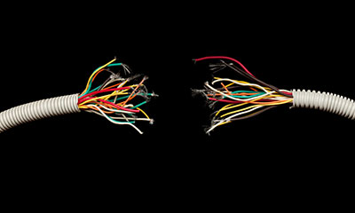
Multilayer printed circuit boards, or MLPCBs, are becoming more and more popular in the world of electronics. And this is because they offer several advantages over traditional single-layer PCBs. In this blog post, we will discuss what MLPCBs are and why they are becoming so popular. We will also explore some of the benefits that they offer over pcb manufacturing companies. Stay tuned for an in-depth look at multilayer PCBs!
Contents
- What are Multilayer PCBs?
- Benefits multilayer PCBs
- Lightweight
- Small in size
- High assembly density
- High Durability
- Higher Performance
- signal transmission
- Increased Efficiency
- Multilayer Board Disadvantages
- Long manufacturing time
- Requiring Professional Designers
- Debugging/Repairing Is Difficult
- Multilayer PCB Applications
- Telecommunications
- Computers and Peripherals
- Consumer Electronics
- Automotive Electronics
- Industrial controls
- Medical Devices
- Aerospace and Defense
- Multilayer Printed Circuit Board Layers Stack up
- Top Layer & Bottom Layer / outer layer ( Electronic Components)
- Inner Layers (Routing)
- conductive layers
- Multilayer PCB Manufacturing Process
- Making the Core of the Inner Layer
- Multilayer PCB lamination Process
- Multilayer PCB Materials
- Multilayer rigid-flexible PCB
- Multilayer rigid-flex board applications
- The Multilayer rigid-flexible PCB pros
- Multilayer PCBs vs Double-Sided PCBs vs Single-layer PCB
- Considerations in Multilayer PCB Design
- Choosing the Right Multilayer PCB Manufacturers
- Summary
What are Multilayer PCBs?
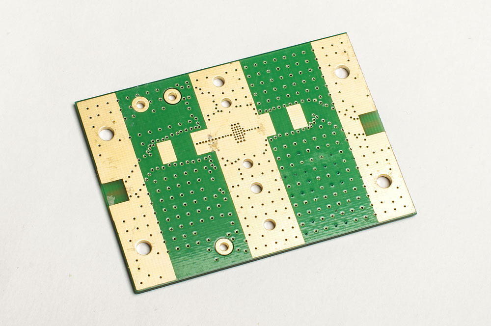
Electronic PCB bottom layer
Multilayer PCB (Printed Circuit Board) is a printed circuit board that has at least three layers of copper foil. Instead of double-layered PCBs, or not a single-layer PCB.
In other words, a Multilayer PCB must have more than two conductive layers of material or copper layer.
The inner layer of the multilayer PCBs must have at least three copper layers, which we will interconnect by copper-plated holes/through-hole plated. However, there are two conductive layers on top and bottom of the PCB substrate in double-layered PCBs.
The plating on the holes between each layer is copper. The layers can be 4, 6, 8...40 in number.
A multilayer PCB is a complicated board by nature. Therefore, the top and bottom layers resemble a double-sided PCB, but they are staked on top of each other with an alternating insulating layer in between.
Also, manufacturers compress each layer to make a single multilayer PCB with copper-plated holes connecting all the layers.
Benefits multilayer PCBs
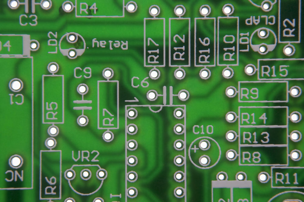
Close Up Of Circuit Board
Multilayered PCBs are common in high-density applications. In this section, we will talk about the main multilayer PCB advantages.
Lightweight
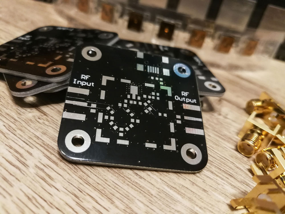
Unassembled radio frequency electronics PCB
One of the multilayer PCB benefits is that these types of boards are thinner and lighter than other types of PCBs. This weight advantage is because multilayer PCBs have fewer layers than other types of PCBs.For example, a multilayer PCB can be as thin as 0.004 inches (0.1016 mm), while a conventional six-layer board can be 0.032 inches (0.81 mm) thick.This weight advantage is extremely important in certain applications, such as aerospace and automotive applications, where every ounce counts.In addition, the multilayer PCB weight advantage also makes these boards easier to handle and less likely to be damaged during assembly and installation.
Small in size
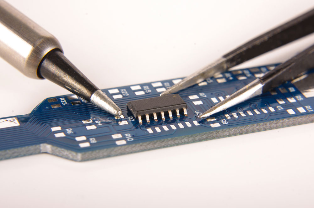
Small electronics integrated circuit IC on empty PCB board ready for hand assembly
Multilayer PCBs are also smaller in size than their counterparts. That's because multilayer boards have more conductive layers per unit area than conventional boards. For example, double-sided boards or single-sided PCBs.
This means that you can use multilayer PCBs to create smaller, more compact electronic devices. Such as smartphones, tablets, and wearable devices.
High assembly density
Multilayer PCBs have a higher assembly density than other types of circuit boards. As a result, multilayer PCBs have more conductive layers per unit area. So this allows for more electronic components to be placed on a multilayer PCB. Therefore, this results in a smaller, more compact overall product.
High Durability
The multilayer boards are more resistant to external factors such as heat, humidity, and physical stress. This is because multilayer PCBs have a stronger structure than other types of circuit boards. Hence, this results in a more durable overall product.
Higher Performance
Multilayer PCBs have a higher performance than other types of circuit boards. This is because multilayer PCBs have a higher density of electronic components. Therefore, this results in a product that can handle more complex electronic signals.
signal transmission
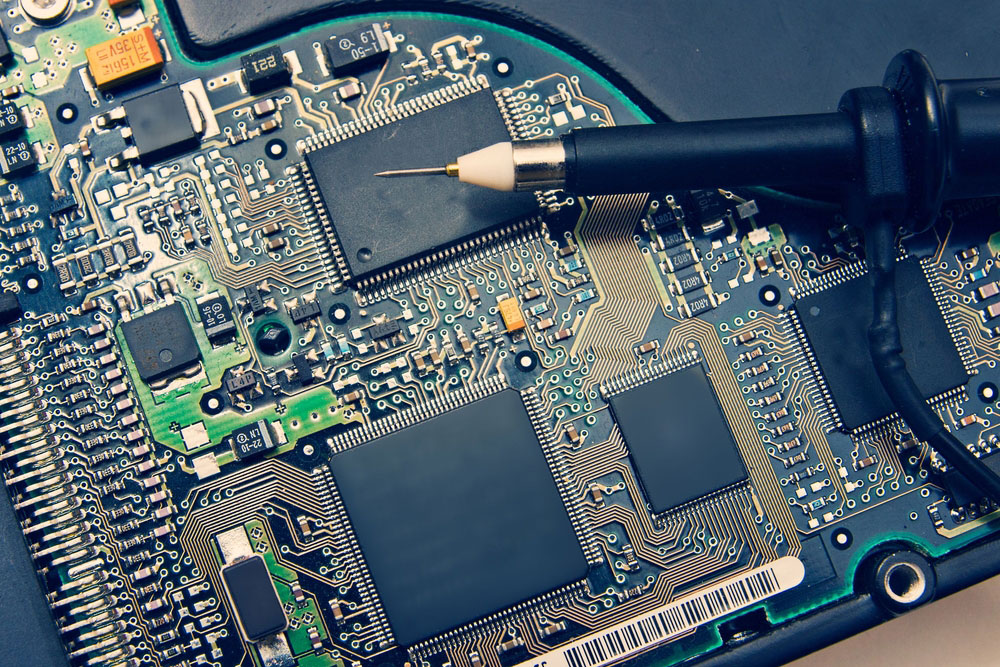
Oscilloscope Probe on Electronic circuit
One of the most important advantages of multilayer PCB is its ability to support high-speed signal transmission. In truth, the multilayer PCB stack provides a low impedance path for the signal to travel. Consequently, this means that multilayer PCB can support data rates of up to gigabits per second.
Increased Efficiency
Multilayer PCBs are more efficient than other types of circuit boards. As multilayer PCBs have more than two layers of electrical connection, you can use them to create smaller and more efficient circuits. In addition, you can also use multilayer PCB to create circuits with higher component densities.
Multilayer Board Disadvantages
Although multiple layers are advantageous, they also come with some disadvantages. Here are some cons:
Long manufacturing time
One multilayer PCB can take up to two weeks to manufacture. And this is because we must make each layer separately and then bond it together.
Therefore, this can be costly and time-consuming, especially for companies that need to produce multilayer PCBs in large quantities.
Requiring Professional Designers
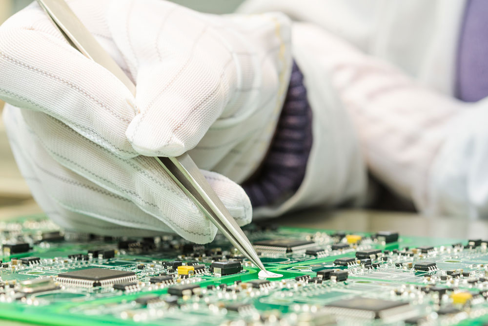
Engineering and electronic component quality control in QC lab on computer PCB turnkey manufacturing
Another disadvantage of multilayer PCBs is that they require professional designers and manufacturers. Because the process of making a multilayer PCB is more complex than making a single-layer PCB or double-sided PCB.As a result, multilayer PCBs can be more expensive to produce.
Debugging/Repairing Is Difficult
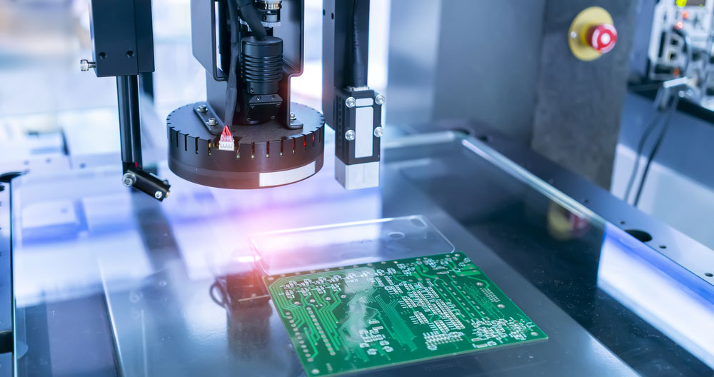
Vision measuring instrument inspecting PCB
If there are any problems with a multilayer PCB, it can be difficult to debug and repair. This is because each layer gets bonded together, making it hard to access individual layers. All the layers also make it difficult to see any issues that might be present.
This can make multilayer PCBs more difficult to work with, especially for those who are not familiar with them.
Multilayer PCB Applications
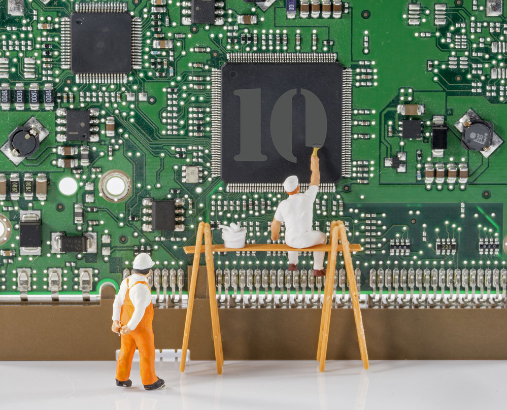
high-speed circuits get ready for windows 10
Multilayer PCBs have become the most common option for a variety of applications in many sectors. Besides, much of this trend is due to continuous pressure toward mobility and functionality across all technologies. Multilayer PCBs make sense as a natural progression, providing more functionality while lowering size. As a result, they've grown quite popular; they're common in
Telecommunications
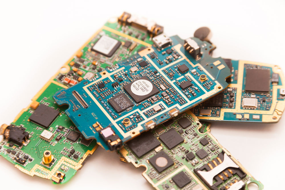
Mobile phones electronic boards
The multilayer PCB is the backbone of modern telecommunications. They are applicable in mobile devices (cell phones), base stations, routers, switches, and many other types of equipment.
Computers and Peripherals
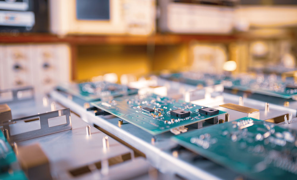
Computer microcircuits in the industrial production of computers
Multilayer PCB is useful in a wide range of computer equipment, from the main board to the smallest peripherals. And others like the following: hard disk drives, CD and DVD drives, modems, printers, etc,
Consumer Electronics

Digital cameras and the city night
You'll find multilayer PCBs in digital cameras, MP players, and other types of consumer electronics. And this makes our life more comfortable and fun.
Automotive Electronics
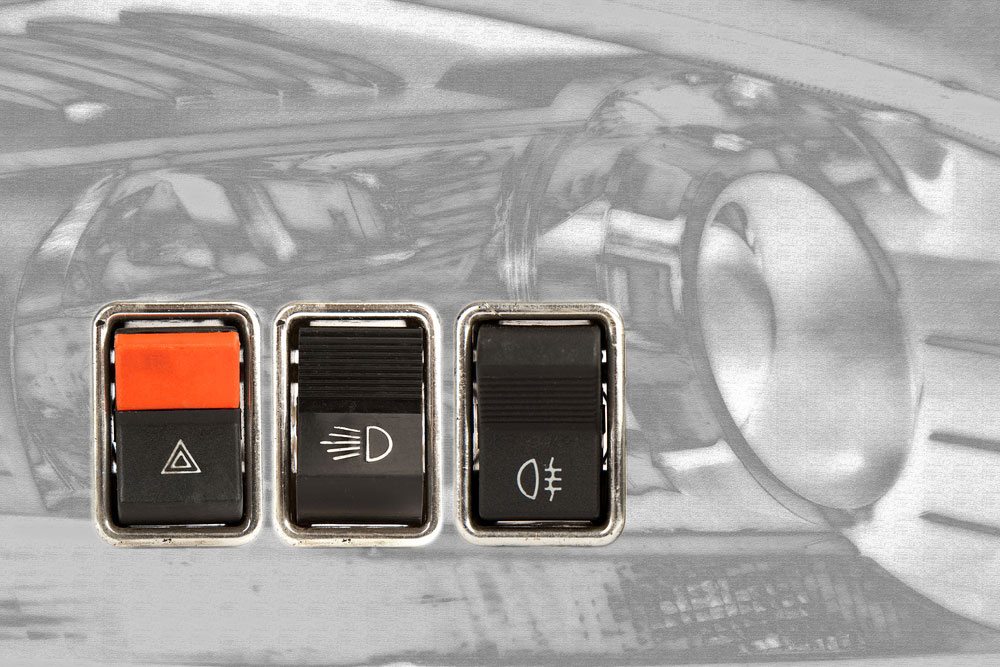
Three car dashboard switches
The automotive industry has embraced multilayer PCB technology. Hence, they are applicable in engine control units, navigation systems, headlight switches, and a variety of other electronic systems in modern vehicles.
Industrial controls
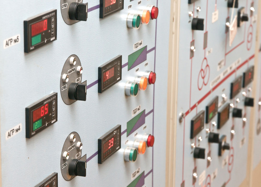
Technical control panel with electric devices
Multilayer PCBs are also commonly in use in industrial control systems. So you may find them in process controllers, programmable logic controllers, and a variety of other industrial control applications.
Medical Devices

Using blood pressure & heart rate monitors
Multilayer PCBs are finding their way into a variety of medical devices. Usually, they are common in everything from blood pressure monitors to MRI machines. Besides, multilayer PCBs are also common in a variety of portable medical devices such as defibrillators and heart rate monitors.
Aerospace and Defense

City map with GPS Icons
Multilayer PCB is also applicable in a variety of aerospace and defense applications. Also, they commonly appear in aircraft flight control systems, guidance systems, and navigation systems. Besides, multilayer PCB is also applicable in a variety of missiles and satellites.
Multilayer Printed Circuit Board Layers Stack up
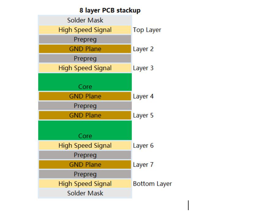
8-layer PCB stack up
The active and passive electrical components are all included on the top and bottom layers.
The inner stacked layers are primarily for routing. Therefore, it's possible to solder through-hole electronic components and Surface Mount Components (SMD) on either side of this design. With Surface Mount Technology and other PCBA Tools, you can solder SMD components.
The following layer stacking is typical for a general multilayer PCBs:
Top Layer & Bottom Layer / outer layer ( Electronic Components)
Layer one and layer two are the top and bottom layers where we will place all the electronic components.
Both of these layers have a thin layer of copper that gets laminated to the dielectric substrate.
The size and shape of the copper traces on these layers will be up to the design of the printed circuit board.
Inner Layers (Routing)
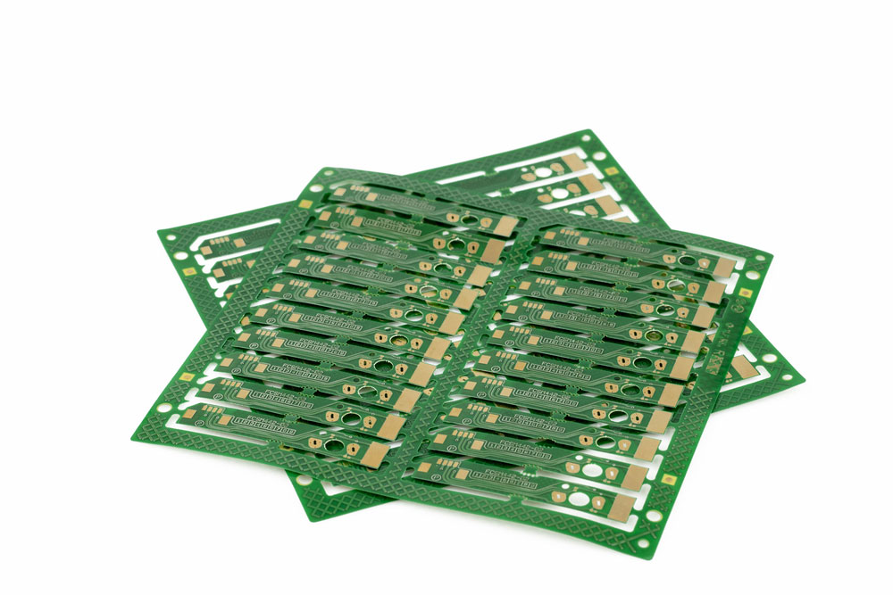
Multiplied PCB boards
Layers three and four are the inner layers where we rout all the interconnecting traces.
These layers also have a thin layer of copper laminated to the dielectric substrate. Also, the copper thickness on these layers is typically much thinner than the top and bottom layers. And this is because the traces on these layers do not have to carry as much current as the traces on the top and bottom layers.
Layers five and six are the inner layers where we rout all the interconnecting traces.
These layers also have a thin layer of copper laminated to the dielectric substrate.
The thickness of the copper on these layers is typically much thinner than the top and bottom layers. Because the traces on these layers do not have to carry as much current as the traces on the top and bottom layers.
conductive layers

Quality test of PCBs on a modern X-Ray equipment inspection system
The conductive layers in multilayered PCBs are part of copper. The copper gets laminated to the dielectric substrate. The thickness of the copper on the conductive layers is typically much thinner than the thickness of the copper on the top and bottom layers. Because the traces on these layers do not have to carry as much current as the traces on the top and bottom layers.
Special Offer: Get $100 off your order!
Email [email protected] to get started!
Multilayer PCB Manufacturing Process
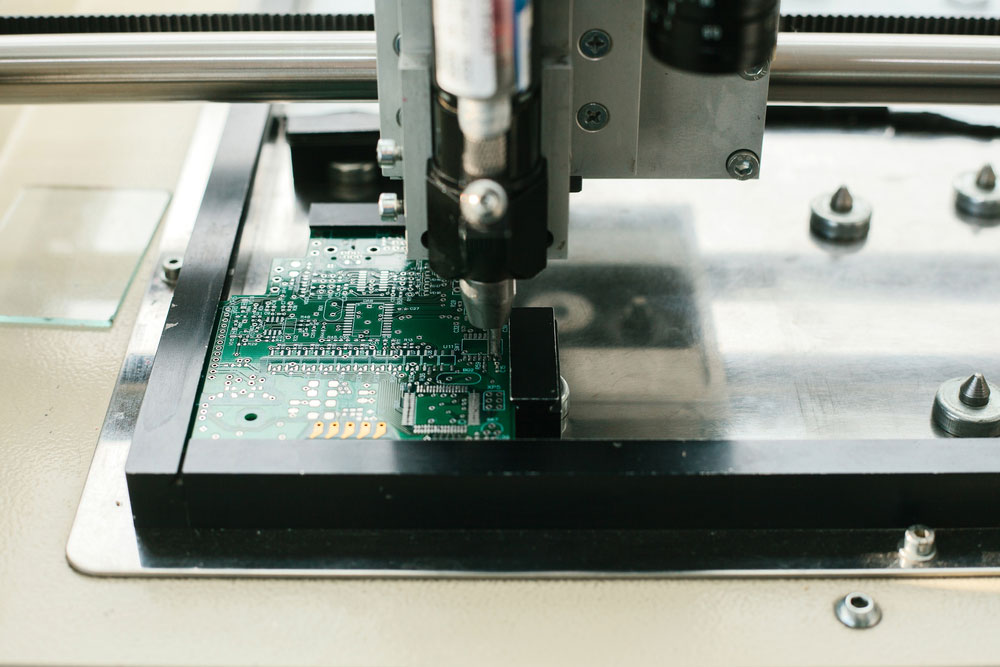
Technological process-assembling the board
The manufacturing process for multilayered PCBs is similar to the process for making double-sided PCBs. First, you deposit a layer of conductive material on each side of an insulating substrate.
Next, sandwich together two or more double-sided PCBs to create the inner layers. Finally, you should add the outer layers, and laminate the entire multilayered PCBs with an insulating material.
Making the Core of the Inner Layer
The Inner layer core is the first step in the manufacturing process of multilayer PCBs. To begin, pick a sheet of laminate with the right thickness and cover it with the required amount of Cu foil.
Cover both sides of the core materials with a "hot-roll" laminated in-place dry film resist and UV-sensitive.
Next, we will transfer the inner layer circuitry and planes to the resist using film, which the electronic data generates. Then the UV light makes direct contact with the resist, hardening it so that it adheres to the core surface.
In the next operation, the light-resistant resist will form away. Offsetting the resist exposes the Cu regions that will remove from the core's surface.
Multilayer PCB lamination Process
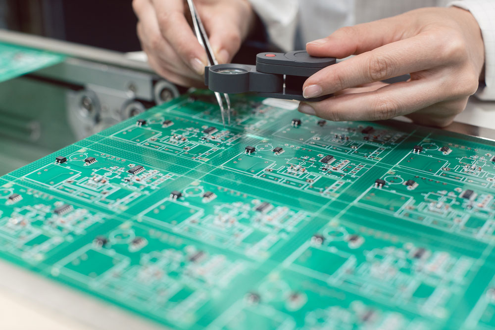
Technician inserting electronic components into a PDB for assembly
The lamination process, which several PCB manufacturers use, utilizes the materials in such a way as the inner layer core, Cu foil sheets, and “prepreg” (woven glass cloth with epoxy resin) sheets.
Next, we will drill the multilayer PCBs. Also, use a CNC machine that has a rotating drill bit to finish this. In addition, the drill bit is precision-guided and makes contact with the multilayer PCB.
After the drilling process is fine, the multilayered PCBs are then ready for the plating process. In this process, you could apply a thin layer of metal to the drilled multilayer PCBs. Besides, this metal is usually copper.
The final step in the multilayer PCB manufacturing process is the solder mask. Usually, the solder mask is a green or black lacquer that is in use for the multilayer PCB. Hence, this protects the multilayer PCB from oxidation and corrosion.
Multilayer PCB Materials
Multilayer PCB material choices are important for many reasons. For example, you choose some multilayer PCB materials for their low dielectric constants, while you may choose others for their low thermal conductivity. In addition, multilayer PCB materials must also have good dimensional stability. And they should be able to withstand the rigors of the multilayer PCB manufacturing process.
There are many different multilayer PCB materials available on the market today. Some of the more popular multilayer PCB materials include:
- - Polyimide
- - Rogers Corporation RO400 Series Laminates
- - Teflon
- - Polycarbonate
- - FR-408HR Laminates
Each of these multilayer PCB materials has its own unique set of properties that make it well fit for use in multilayered PCBs. In general, multilayer PCB materials must have good dielectric properties, good mechanical strength, and good thermal stability.When selecting a multilayer PCB material, it is important to consider the intended use of the multilayer PCB. For example, multilayer PCB materials that are applicable in high-temperature applications must be able to withstand temperatures that exceed 300°C.It is also important to consider the manufacturability of the multilayer PCB material. For example, some multilayer PCB materials are difficult to fabricate and require special processing techniques.
Multilayer rigid-flexible PCB
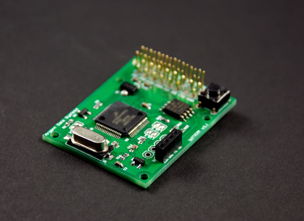
Electronic components and devices
Multilayer rigid-flexible PCBs are multilayer PCBs that have a rigid section and a flexible section. Also, the rigid section is typically made of FR-42 material, while the flexible section is in uses polyimide.
Multilayer rigid-flex board applications
The multilayer rigid-flexible PCB is common in a variety of applications, including:
- - Avionics
- - Military electronics
- - Medical electronics
- - Telecommunications
The Multilayer rigid-flexible PCB pros
Multilayer rigid-flexible PCBs offer several advantages over traditional multilayer PCBs, including:
- - Increased flexibility
- - Increased durability
- - Reduced size and weight
- - Improved performance in harsh environments
Multilayer rigid-flexible PCB is the future of electronics. With their many advantages, they are sure to become increasingly popular in a wide variety of applications.
Multilayer PCBs vs Double-Sided PCBs vs Single-layer PCB
Multilayer PCBs are made up of multiple layers of conductive material, typically alternating between insulating and conductive layers. Double-sided PCBs have two conductive layers, while single-layer PCBs only have one.
In addition, multilayer PCBs offer many advantages over double-sided and single-layer PCBs, including increased flexibility, increased durability, reduced size and weight, and improved performance in harsh environments.
While multilayer PCBs offer many advantages, they also come with some disadvantages. For example, they are more expensive than double-sided or single-layer PCBs, and they are more difficult to manufacture. In addition, multilayer PCBs are not as widely available as double-sided or single-layer PCBs.
Despite the disadvantages, multilayer PCBs are the future of electronics. They offer several advantages that make them well suited for a wide range of applications. As the technology continues to improve, multilayer PCBs are likely to become even more popular in the years to come.
Considerations in Multilayer PCB Design
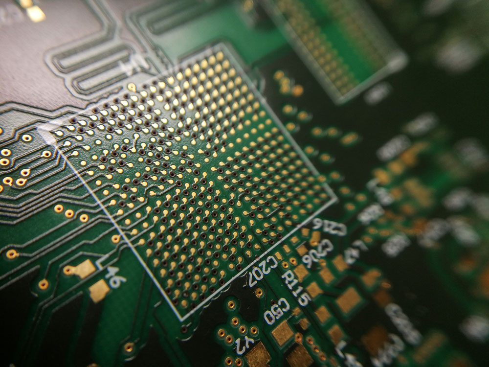
Macro close-up of BGA ball grid array technology footprint on electronic board
There are several things to consider while designing your Multilayer PCBs. For example, the number of layers, the thickness of the copper foil, the dielectric constant of the insulating material, and so on.You should also keep in mind that multilayer PCBs are more expensive to manufacture than conventional printed circuit boards. This is because they require specialized equipment and processes.However, the benefits of multilayer PCBs far outweigh the cost. They offer greater flexibility in design, better electrical performance, and improved reliability.
Choosing the Right Multilayer PCB Manufacturers
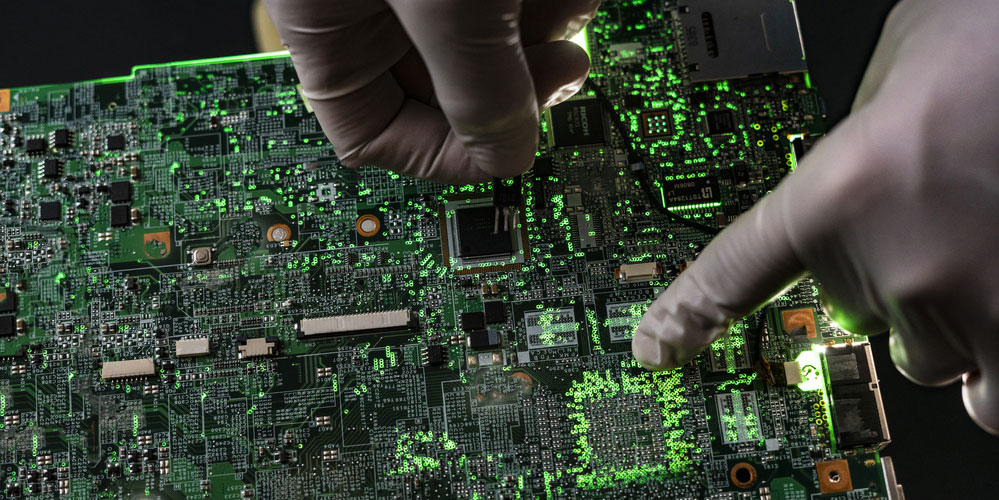
Manufacture of the new modern micro electronic technology computer boards
When choosing multilayer PCB manufacturers, it is important to consider the following factors:
- - The experience of manufacturers in manufacturing multilayer PCBs.
- - The manufacturers' ability to provide multilayer PCBs with the desired features and specifications.
- - The price for multilayer PCBs.
The multilayer PCB manufacturing process is also an important factor to consider when choosing multilayer PCB manufacturers. For example, some multilayer PCB processes are not compatible with certain multilayer PCB materials. In addition, manufacturers should also be able to provide the multilayer PCB material with the desired properties.
Summary
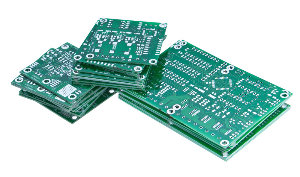
Stacked circuit boards
Multilayer printed circuit boards (PCBs) are the future of electronics. They offer many advantages over single and double-sided PCBs, including improved performance, smaller form factors, and reduced costs.
However, multilayer PCBs are more complex to design and manufacture than their single and double-sided counterparts. This guide will explain what multilayer PCBs are, how they work, and their advantages and disadvantages. If you have any questions about multilayer PCBs, please contact us. Thank you for reading!
Special Offer: Get $100 off your order!
Email [email protected] to get started!


