Blog  /  Hole Diameter: How to Calculate the Hole Size

Hole Diameter: How to Calculate the Hole Size

At OurPCB, we understand the importance of precise hole diameter calculations in PCB manufacturing. The difference between non-plated and plated through-holes can affect the overall performance of the board. Our PCB manufacturing service ensures accurate hole dimensions to meet your specifications, enhancing the reliability of your electronic products.
Quote Form
check whiteFast Turnaround check whiteISO Certified
1 2 3

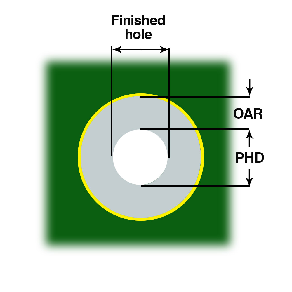
A hole diameter or PHD refers to a production tool’s diameter that you use to drill holes.

So, the calculation of a hole size diameter differed for non-plated through holes and plated through holes.

For a non-plated through-hole, the calculation is the sum of the finished hole size and +0.00mm/0mil.

But, plated through-hole, on the other hand, is the sum of the finished hole size and +0.10mm/4mil.
 

 Hole Diameter

PCB hole diameter


Special Offer: Get $100 off your order!

Enjoy $100 off your order! No hidden fees and no minimum order quantity required.
Email [email protected] to get started!

Production Holes Diameter/PHD


The calculation for the PHD =

  1. Finished hole size + 0.00mm/0mil for Non-Plated Through Holes
  2. Finished hole size +   0.10mm/4mil for Plated Through Holes
  3. PHD – finished hole size = copper plating finish + applied finish


 Hole Diameter--OAR (Outer layer Annular Ring)


The OAR is the outer layer annular ring. And you can calculate it by dividing the difference between the copper pad diameter and tool size by 2.

Hole Diameter


FAR (Finished Annular Ring)

The Finished Annular Ring is the part that lies between the solder hole and the external solder pad rim.

Plus, the annular ring breaks when the drilled hole is off the center.

But it's all dependent on the external diameter of the solder pad against the nominal hole size diameter.

Calculation of FAR;

The width (T1) of the finished annular ring on external layers should be >= 0.050 mm for the board.

The width (t2) of the annular ring on inner layers should be >= 0.0100 mm for the board.


Special Offer: Get $100 off your order!

Enjoy $100 off your order! No hidden fees and no minimum order quantity required.
Email [email protected] to get started!
Hommer Zhao

Hommer Zhao, based in Shenzhen, China, founded OurPCB in 2005, a PCB Manufacturing company.

As a regular contributor to Circuit World and the Journal of Manufacturing Systems, Hommer shares expertise on advanced PCB fabrication processes. His research on manufacturing optimization appears in the International Journal of Production Research and Journal of Industrial Information Integration.

Serving on the Indian Printed Circuit Association (IPCA) advisory board, Hommer Zhao frequently presents at technical seminars and industry exhibitions. He maintains strong partnerships with leading institutions including UCL's Electronic Engineering Department and their PCB prototyping facilities. Under his leadership, OurPCB has pioneered enhanced PCB manufacturing machining capabilities for high-precision PCB manufacturing, particularly serving telecommunications, automotive, and medical device sectors.

Table of Contents

Related Post