


ISO 9001/UL Certified
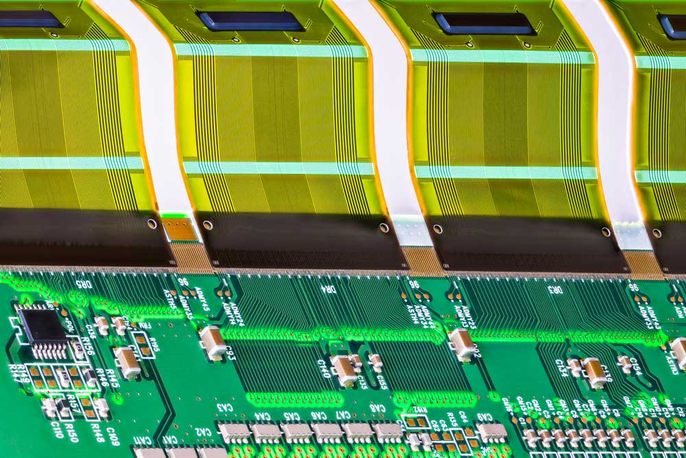
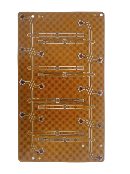
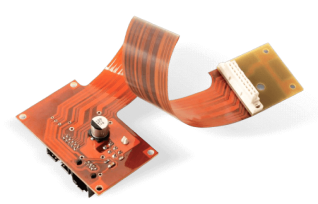
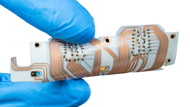
PCB Assembly Specialists
97% of PCB Shipped on Time
98% of PCB Delivered to Spec
Delivery Guarantee

Online Quote

Upload PCB File

Order Review

Payment

Order Updates

Delivery

Confirm Received


Laminate Formation & Preparation
- Step 1: Fabricate flexible laminates by bonding copper to PI film
- Step 2: Laminate coverlay and copper foil
Drilling & Plating
- Step 3: Drill holes for vias and through holes
- Step 4: Electroplate holes to form conductive vias
Circuit Patterning
- Step 5: Image and develop photoresist for circuit pattern
- Step 6: Etch away unwanted copper
- Step 7: Strip photoresist and apply solder mask over bare copper
Solder Mask & Surface Finish
- Step 8: Expose and develop a solder mask
- Step 9: Cure solder mask and apply surface finish
Shaping & Marking
- Step 10: Punch or route PCB to final shape
- Step 11: Print silkscreen legends and conduct electrical tests
Final Processing & Packaging
Step 12: Singulation and packaging
Chat with Us
Mon-Fri: 24 hours,
Sat: 9am-6pm, GMT+8
Email Us
Reach us at
[email protected]
24 hours online
Call us
+86-199-30589219
Mon-Fri: 24 hours,
Sat: 9am-6pm, GMT+8

