


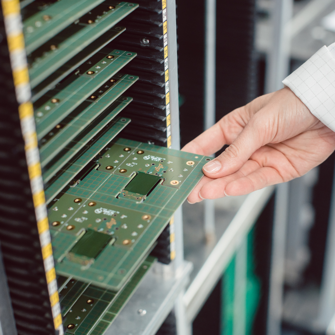
- Rigorous testing at every production stage
- IPC standard compliance for reliable performance

- Premium equipment for precise fabrication
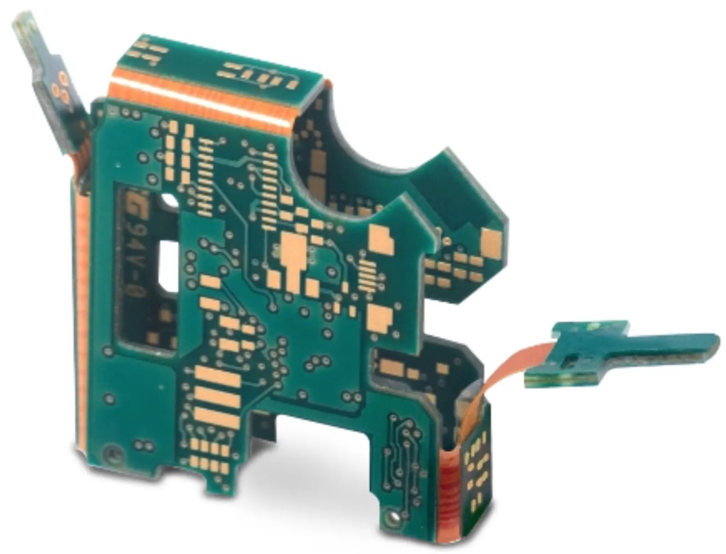
- Capability to handle complex designs and tight tolerances

- Dedicated team for personalized assistance
- Quick response to inquiries and design modifications

- Cost-effective solutions without compromising quality
- Volume discounts for larger orders

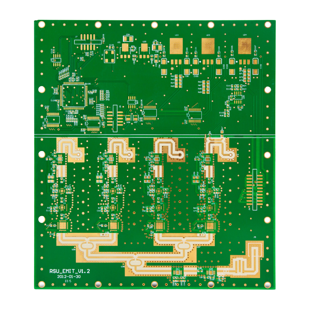
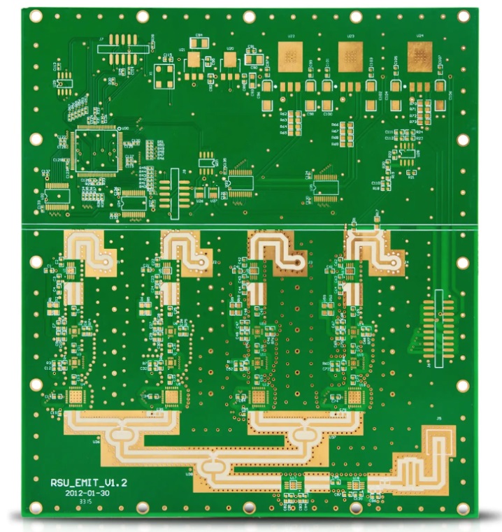
- Dedicated ground and power planes reduce noise
- Better control over impedance and crosstalk

- More routing options in a compact form factor
- Ideal for designs with moderate component density

- Better shielding against EMI
- Reduced emissions for improved product compliance

- Allows for mixed-signal designs on a single board
- Supports both through-hole and surface-mount components

We use advanced Surface Mount Technology for high-density, compact designs. Our SMT lines handle a wide range of component sizes and types. This process is ideal for modern, space-constrained electronic products.

We adapt to your needs. You can provide components, or we can source them for you. Our turnkey service covers everything from part procurement to final assembly. This flexibility helps streamline your production process.

Every project is unique. We tailor our assembly process to your specific requirements. Our team works closely with you to understand and implement your design intent. This ensures the final product meets your exact needs.

Time is often critical in electronics development. We offer fast turnaround options without sacrificing quality. Our efficient processes and dedicated teams make quick deliveries possible. This helps you meet tight project deadlines.

For high-reliability applications, we offer IPC Class 3 assembly. This standard is crucial for aerospace, medical, and other critical industries. Our strict quality controls ensure these demanding requirements are always met.

We have expertise in assembling all types of IC packages. This includes BGAs, QFNs, and other complex components. Our advanced equipment and skilled technicians ensure precise placement and reliable connections.
Mon-Fri: 24 hours,
Sat: 9am-6pm, GMT+8
Reach us at
[email protected]
24 hours online
+86-199-30589219
Mon-Fri: 24 hours,
Sat: 9am-6pm, GMT+8

