


- Assistance with stackup optimization for improved signal integrity
- Guidance on material selection for specific performance requirements

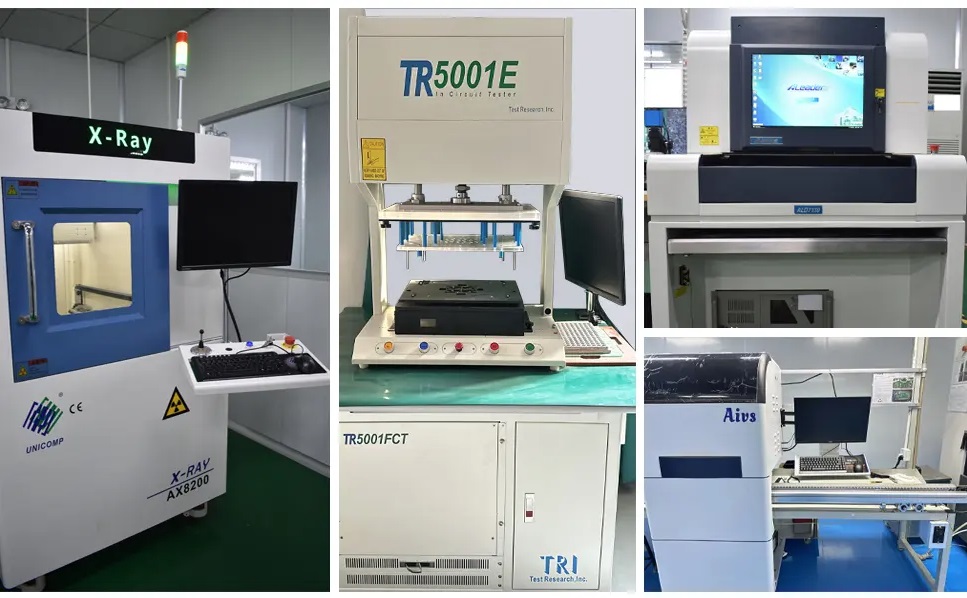
- High-quality equipment for precise layer alignment
- Rigorous quality control processes at every production stage

- Quick-turn prototyping services for faster time-to-market
- Scalable production capacity to meet varying order volumes

- In-house electrical testing to ensure board functionality
- Compliance with industry standards and regulations

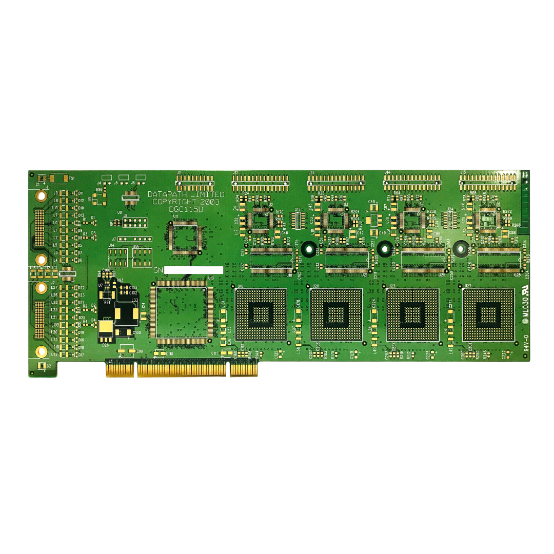
- More layers allow for higher component density
- Enables miniaturization of electronic devices

- Better control over electromagnetic interference
- Reduced crosstalk between signal traces

- Dedicated power and ground planes for stable voltage supply
- Improved thermal management in high-power applications

- More routing options for complex circuit layouts
- Ability to separate high-speed and low-speed signals

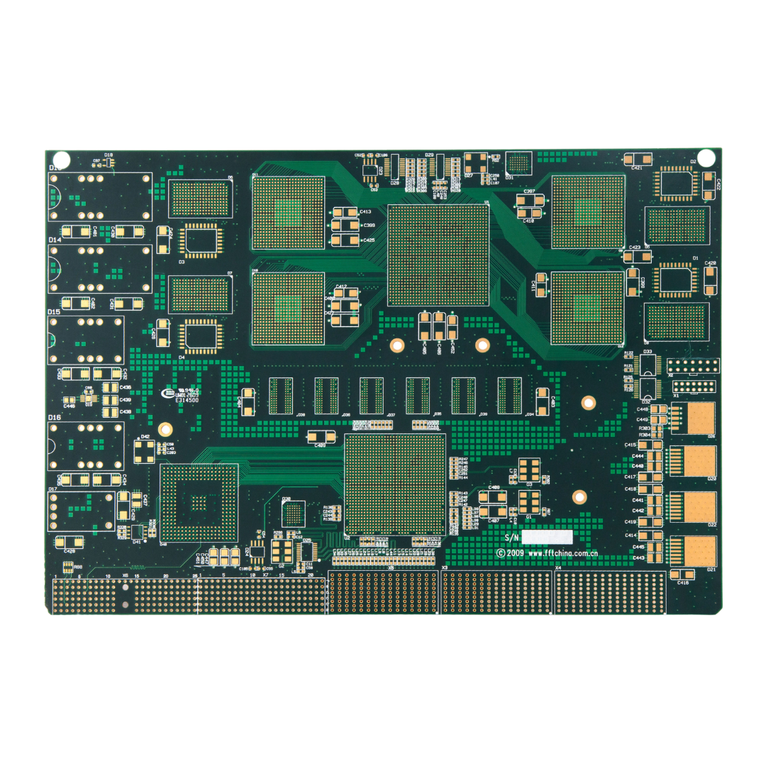

- More layers allow for higher component density
- Enables miniaturization of electronic devices

- Better control over electromagnetic interference
- Reduced crosstalk between signal traces

- Dedicated power and ground planes for stable voltage supply
- Improved thermal management in high-power applications
- More routing options for complex circuit layouts
- Ability to separate high-speed and low-speed signals

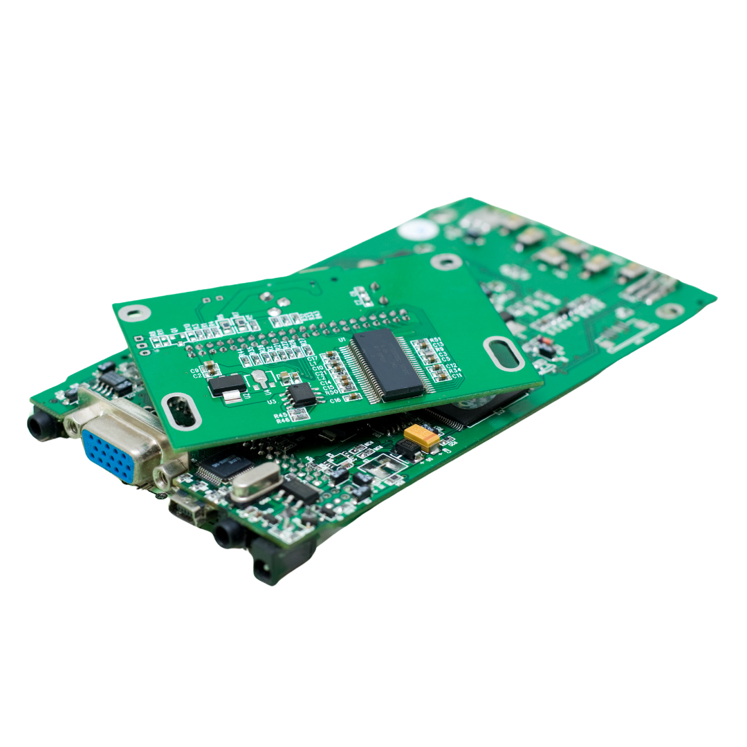
We use Surface Mount Technology for high-density, compact PCB assemblies. Our SMT process ensures precise component placement and reliable solder connections.

We accommodate both customer-supplied components and full turnkey solutions. Our turnkey service covers component sourcing, assembly, and final delivery.

Our team works closely with clients to deliver tailored assembly solutions. We adapt our processes to meet unique design requirements and specifications.

We offer fast turnaround times without compromising quality. Our efficient processes enable rapid prototyping and small-batch production.

We adhere to strict IPC Class 3 standards for high-reliability applications. This service is ideal for aerospace, medical, and other critical industries.

We have expertise in assembling various IC package types. This includes BGA, POP, CGA, QFN, DFN, and CSP components.
Mon-Fri: 24 hours,
Sat: 9am-6pm, GMT+8
Reach us at
[email protected]
24 hours online
+86-199-30589219
Mon-Fri: 24 hours,
Sat: 9am-6pm, GMT+8

