


ISO 9001/UL Certified
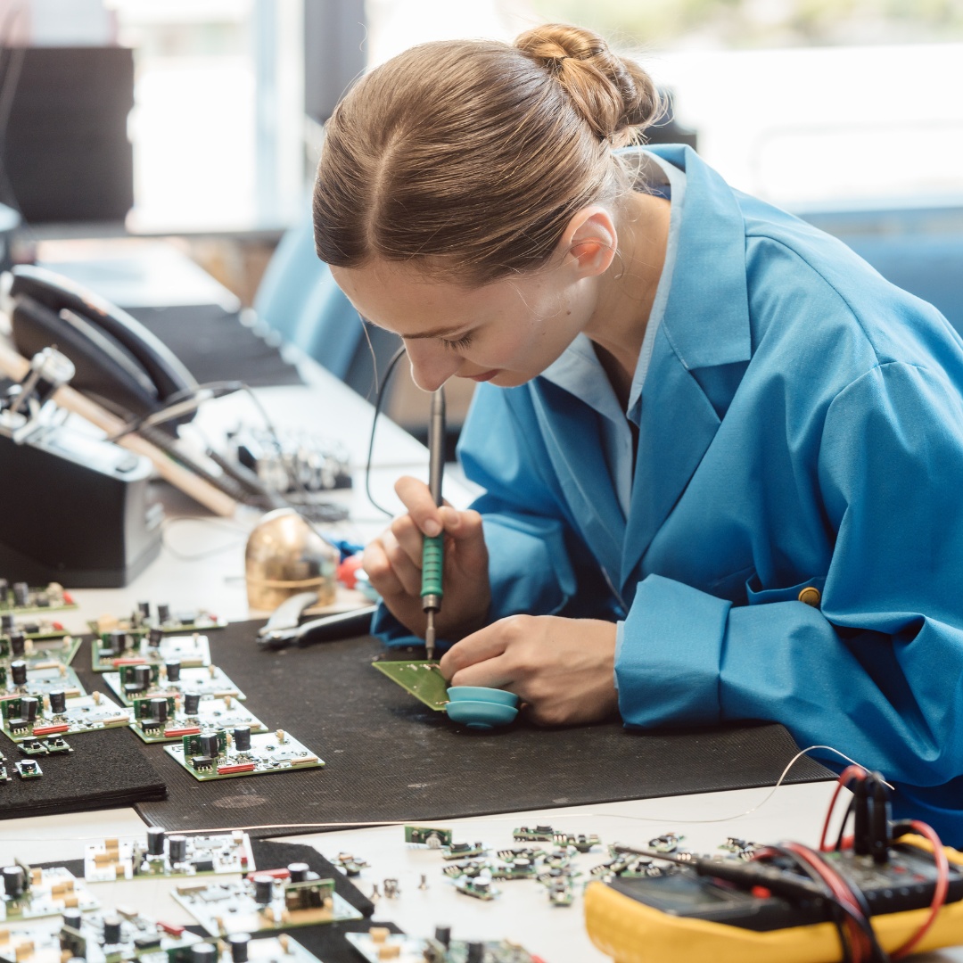
PCB Assembly Specialists
97% of PCB Shipped on Time
98% of PCB Delivered to Spec
Delivery Guarantee

Online Quote

Upload PCB File

Order Review

Payment

Order Updates

Delivery

Confirm Received


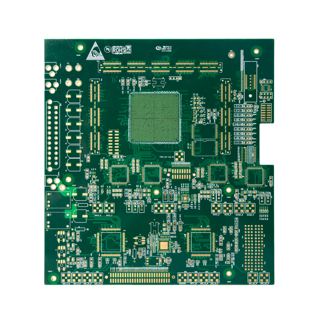
Complex Layer Stacking
- Precise layer alignment
- Controlled impedance with ±10% tolerance


Advanced Production
- Sophisticated via structures
- Fine line capabilities

Thorough Testing
- Advanced AOI inspection
- X-ray verification

Advanced Technology
- OurPCB uses premium equipment to manufacture insulated metal substrate PCBs
- Exceptional precision and consistency

Quality Assurance
- Every IMS board undergoes rigorous testing
- Automated optical inspection (AOI) and thermal analysis
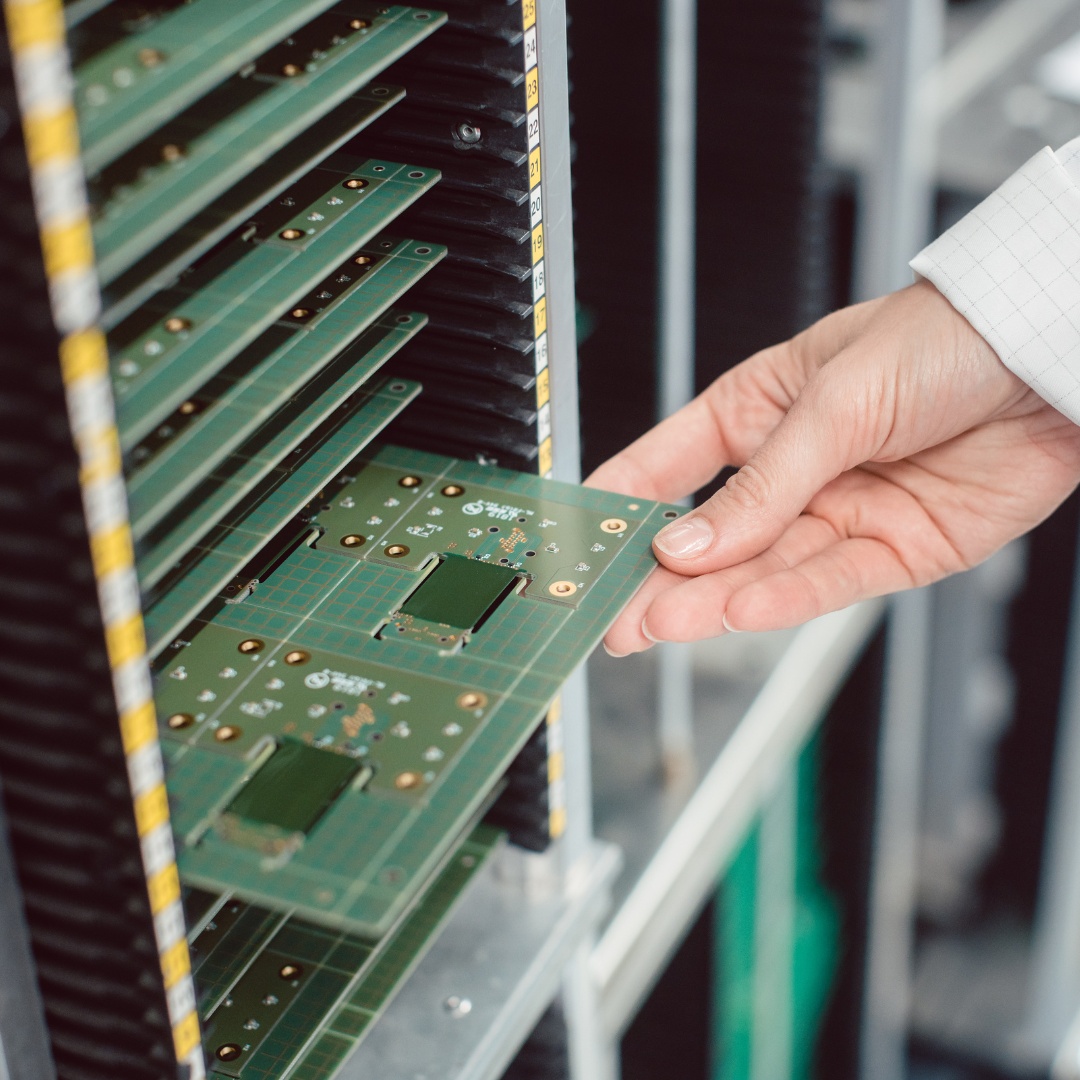
Custom Solutions
- We design tailored solutions to meet unique project requirements
- OurPCB handles both multilayer and single-sided IMS boards
Proven Reliability
- Years of experience serving global industries
- OurPCB has a strong reputation as a trusted MCPCB manufacturer

High-Density Fabrication
- Fine trace capabilities
- Advanced interconnect options

Material Engineering
- Application-specific substrate selection
- Thermal management solutions

Specialized Construction
- Choose from blind and buried vias
- Controlled dielectric thicknesses

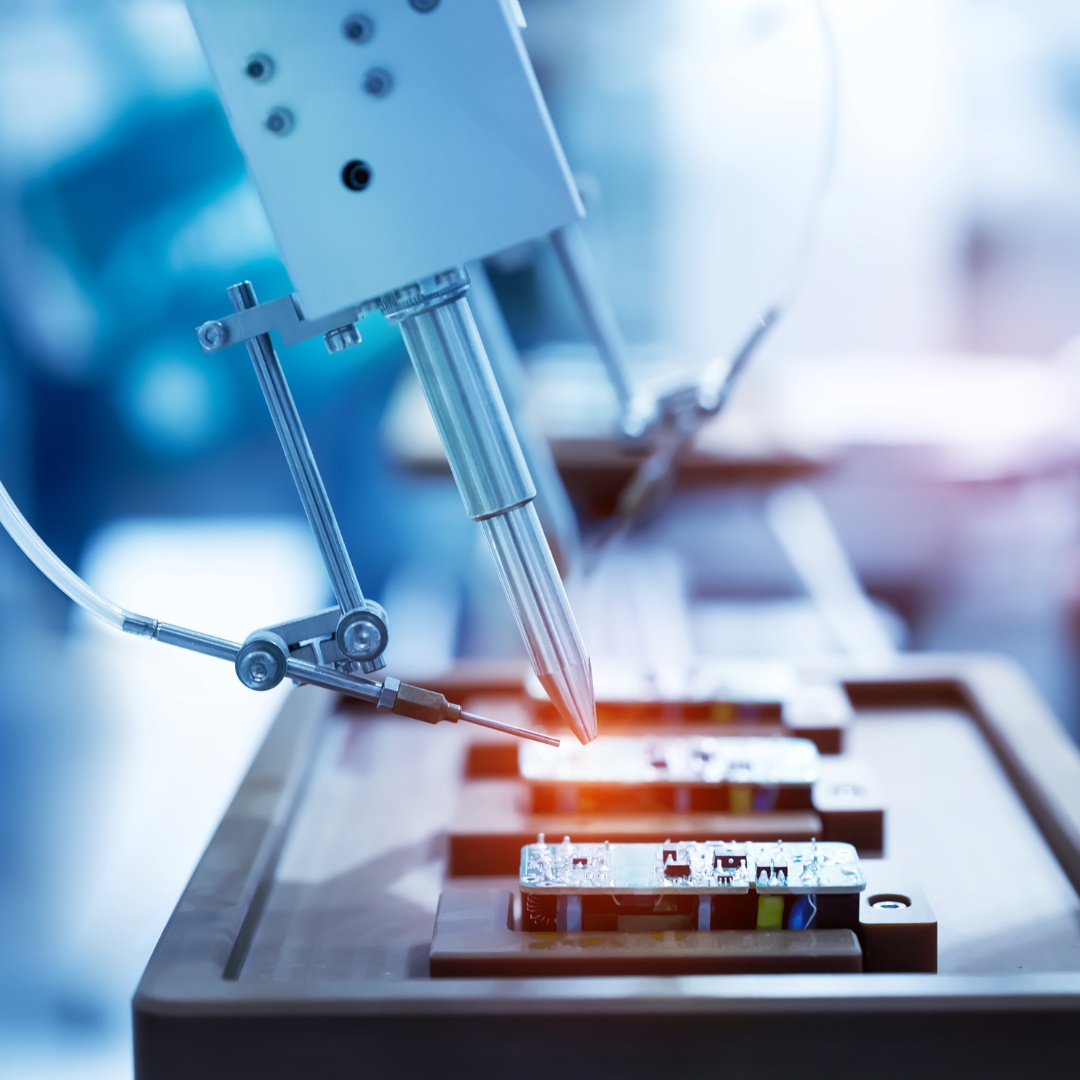
PCB Assembly Services
- Full PCBA services
- Original component sourcing

Comprehensive Testing
- Electrical performance verification
- Signal integrity validation

High-Quality Protective Finishes
- Multiple surface finish options
- Application-appropriate selections
Chat with Us
Mon-Fri: 24 hours,
Sat: 9am-6pm, GMT+8
Email Us
Reach us at
[email protected]
24 hours online
Call us
+86-199-30589219
Mon-Fri: 24 hours,
Sat: 9am-6pm, GMT+8

