Do you want to solder electronic components on your printed circuit board quickly? Do you find it time-consuming to solder them using the soldering irons manually?
It is also unsafe to inhale smoke for a long time. So, who would not want to look for an alternate way of soldering?
You just got lucky, as there is another standard way of soldering that is super quick. Can you guess what we are talking about? It is a wave soldering!
This process of soldering will allow you to make several printed circuit boards in a short time. So, this article is all about wave soldering. Stay put.
Contents
- 1、Wave Soldering
- 1.1 What is Wave Soldering?
- 1.2. Technical Details about Wave Soldering
- 1.3 When to use Wave Soldering?
- 2、Wave Soldering Process
- 2.1 Wave Soldering Machine
- 2.2 Wave Soldering Temperature
- 2.3 Fluxing
- 2.4 Preheating
- 2.5 Cleaning
- 3、Types of Soldering
- 3.1 Dip Soldering vs. Wave Soldering
- 3.2 Reflow Soldering vs. Wave Soldering
- 4、Selective Wave Soldering
- 4.1 Selective Soldering Machine
- 4.2 Selective Wave Soldering Guidelines
- 4.3 Selective Soldering problems
- 4.4 Selective Wave Soldering Machine Cost
- 5、Wave Soldering Defects and Problems
- 5.1 Wave Soldering Defects and Problems
- 5.2 Cost
- 6、Conclusion
1、Wave Soldering
1.1 What is Wave Soldering?
Back in the days when surface mount technology was not entirely developed, "wave soldering" was a very famous soldering technique.
Nearly every PCB used wave soldering for the placement of electronic components. Wave soldering is a mass soldering procedure that will permit you to make many PCBs quickly.
You will need to pass every PCB over a pan of liquefied solder. There, a pump will create a surge of solder that will resemble a standing "wave."
This standing wave shows over the printed circuit board, and the electronic components will be soldered to the PCB. So, the contact between the solder and the lock does the magic.
After that, the printed circuit board gets blowing air or water spray for safe cooling. This cooling process will secure the components in their place.
Furthermore, wave soldering is usually done in a shielding gas environment, as nitrogen usage helps mitigate solder defects. Figure 1 shows electronic components placed on PCB and all ready to go under the soldering machine.
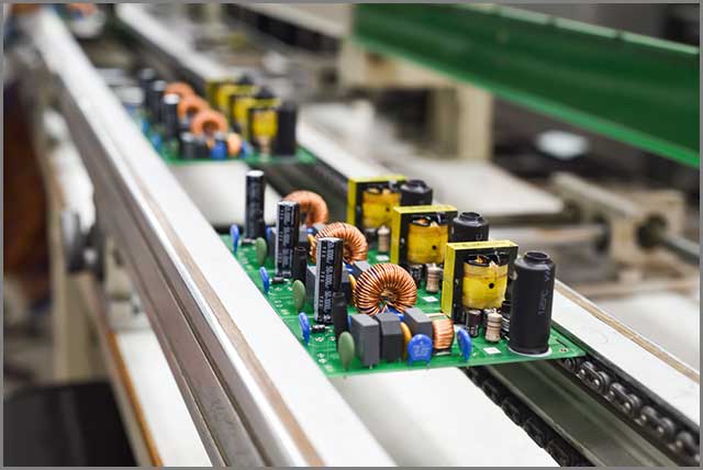 Image 1: Soldering Process
1.2. Technical Details about Wave Soldering
Technically, this soldering process utilizes a whole tin container for welding. It can go through high temperatures, which melt its bar, and molten tin is formed.
The liquefied tin is taken as "lake water." It is called a "leveling wave" when the lake is static and horizontal. And, It is called a "spoiler wave" when there are waves in the lake.
The printed circuit board can be considered a boat. It will float over the rough or calm lake, permitting the tin to attach electronic parts to the board.
After the tin bath, you will see that it will cool rapidly, and the solder will do its job. And what is that? Of course, it will solder the electronic components to the PCB.
Moreover, you should make sure that temperatures are adequate during this process. If temperature control is not enough, the circuit board can experience mechanical stress.
That, in turn, will lead to conductivity loss and cracks. And a low soldering temperature can cause improper solder thickness, further leading to board stress.
1.3 When to use Wave Soldering?
Wave soldering can be used for surface mount and through-hole printed circuit board assemblies. In surface mount, you must glue electronic components onto the PCB surface using placement equipment. After that, it will be ready to pass via the liquefied solder wave.
In general, wave soldering is mostly used for welding through-hole electronic parts. Hence, in many large-scale applications, where surface mount components are used primarily, you can use reflow soldering instead of wave soldering.
Now you must be wondering what reflow soldering is. Don't worry; we will get to it shortly.
However, you can always use wave soldering for applications that broadly use through-hole components.
We hope that by now, you know the basic concept of wave soldering. In the next chapter, we have described the wave soldering process in detail.
2、Wave Soldering Process
2.1 Wave Soldering Machine
In the market, you will encounter many kinds of wave soldering machines. You can buy lead wave solder machines or lead-free wave solder machines. It is all up to you.
However, the main principles and fundamental parts of these machines are alike. A conveyor is an essential part that is used during this process. It takes printed circuit boards via various zones.
Next, you will see a pan of the solder and pump responsible for generating the primary wave. Furthermore, you will also get a flux sprayer and a preheating pad.
Hence, these four main parts make up a soldering machine. The solder in wave soldering machines is mostly made of a metal mixture.
If the machine has led solder, it will contain 49.5% lead, 50% tin, and 0.5% antimony.
However, in the latest devices, lead-free models are available due to health concerns. So, tin-copper-nickel and tin-silver-copper alloys are frequently used. Figure 2 illustrates a wave soldering machine.
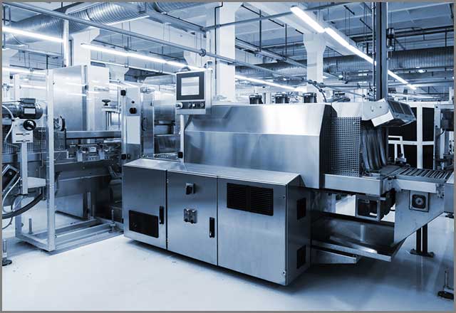 Image 2: Wave Soldering Machine
2.2 Wave Soldering Temperature
Currently, tin alloys for soldering regularly use Sn 60/Pb40 and Sn 63/Pb37. Therefore, it is recommended that you should make sure that the operating temperature stays around 260° ± 5°C.
Nonetheless, it would be best if you also considered the overall weight of the PCB and the parts.
Practically, heavy components can be heated up to 280°C. Lightweight components, which are heat-sensitive, can be heated at a temperature as low as 230 °C.
Further, it would help if you also considered preheating and the conveying speed. Figure 3 shows a close-up of the melting tin.
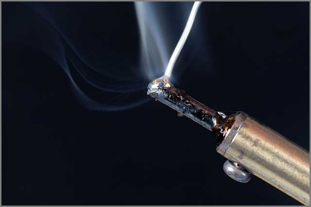 Image 3: Wave Soldering
However, it is best to change the conveying speed rather than the tin's temperature because the temperature change will damage the solder joints' quality by affecting the fluidity of the liquefied container.
At high welding temperatures, copper will start to dissolve, which will ruin overall soldering quality control.
2.3 Fluxing
You should apply liquid flux on the printed circuit board surface during the wave soldering. You will observe that fluxing will enhance the soldering quality of the electronic components.
When stored, these components, printed circuit boards, and also in liquid are exposed to the atmosphere. This exposure can make them oxidized and thus affects the soldering quality.
Flux mainly removes dirt and oxides on the surface of the metal. Further, it also creates a film to stop the air from reacting with the metal surface during a high-temperature setup.
Thus, solder cannot get oxidized easily. Nonetheless, it would help if you used the liquefied tin for soldering during the wave soldering process.
Currently, the melting point of the SAC305 lead-free solder is around 217 °C. And the flux cannot be exposed to such a high temperature for long. Hence, if you wish to use change, you should add it before the printed circuit board goes through the tin solution.
Commonly, flux can be applied by two means. First, you can use a foaming change, and second, you can add it by spraying. In foaming flux, the flux gets attached to the circuit board, which passes through it.
The major downside of this way is that you may observe that change is not uniformly applied. Thus, poor soldering can happen in areas where flux doesn't exist.
In the spraying method, the flux is sprayed through the nozzle as the circuit board passes. The drawback of this method is that the change can be quickly given through the board gaps.
Further, if the change is not processed and only dropped straightly on the board, you can also observe the corrosion of the board. And flux can also directly pollute the electronic components of the circuit board's front.
2.4 Preheating
Normally, Preheating before the primary wave welding process begins. It can increase the upper plate's temperature to between 65 and 121°C with a heating rate between 2 °C /s and 40 °C /s.
You will not be able to get the best soldering results if preheating is insufficient. It is because flux may not reach every part of the PCB. On the other hand, if you set a very high temperature for preheating, "no-clean" flux can suffer. We have explained it in the next sub-section if you wonder what exactly a "no-clean" change is.
2.5 Cleaning
The cleaning process washes a PCB with deionized water or solvents to remove flux remains. However, there exists a kind of flux that doesn't need cleaning.
Can you guess which one? Yes, of course, the "no-clean" changes, their remains after the soldering process, are benign.
But it would help if you were careful; some applications do not want "no-clean" fluxes. It is only because "no-clean" changes can be susceptible to the conditions of the process.
Now that you know all about the wave soldering process. The coming chapter will relate wave soldering with other types of soldering.
Special Offer: Get $100 off your order!
Email [email protected] to get started!
3、Types of Soldering
3.1 Dip Soldering vs. Wave Soldering
In simplest terms, dip soldering is a soldering process with limited scope. Like wave soldering, it can be used for surface mount and through-hole circuit board assemblies.
Further, the solder rains over the bare metallic areas of the printed circuit board. Thus, you will observe a reliable electrical and mechanical connection. Finally, dip soldering is the manual version of the automatic soldering process.
3.2 Reflow Soldering vs. Wave Soldering
Reflow soldering is the most famous way of fixing surface mount components onto the printed circuit board. Creating a solder paste out of flux and solder powder would be best. And then, you will use that paste to fix electronic components onto the contact pads.
You will heat the package under an infrared lamp or reflow oven. The solder will then liquefy and make connections between the joints.
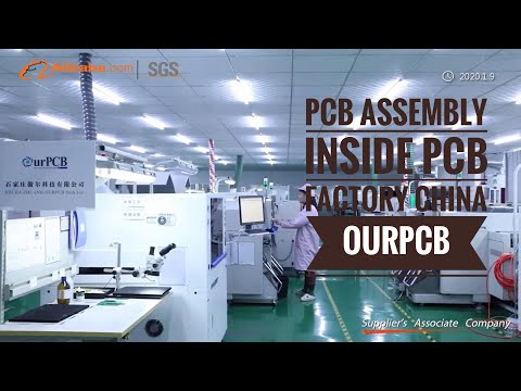
On the other side, you can also solder different joints with a hot air pencil. Figure 4 shows the printed circuit board assembling and moving into the reflow oven machine.
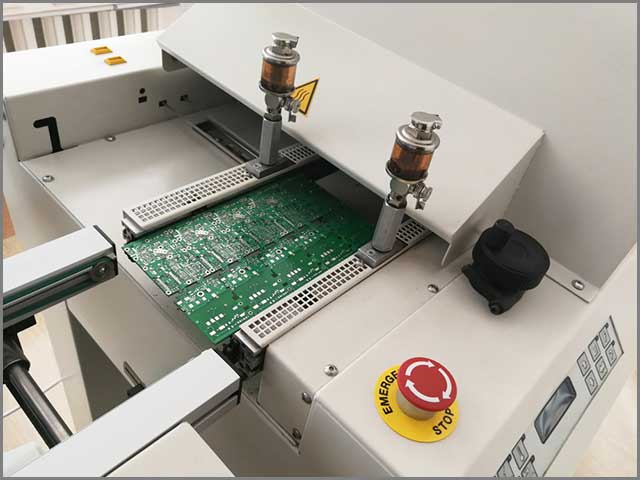 Image 4: Wave Soldering
Now, you must be wondering which technique should be used and when? Generally, wave soldering is more complicated than reflow soldering.
In wave soldering, the time for the PCB stays in the solder wave, and PCB temperature requires careful monitoring. The printed circuit board can be defective if the soldering environment is not right.
However, with reflow soldering, you don't need to fret much about environmental control. In many applications, wave solder is the only useful way of soldering components onto the board.
But with this being true, you must know that wave soldering is cheaper and faster than reflow soldering.
You will notice that reflow is mostly used for small-scale applications. Such applications do not need reliable, cheap, and fast mass production of PCBs.
Surprisingly, you can also use a combination of reflow and wave solder. You can solder components on one side with wave soldering and can use reflow soldering on the other side.
So, these are some alternatives to wave soldering. However, there is still another type of soldering technique that the next chapter compares with wave soldering.
4、Selective Wave Soldering
4.1 Selective Soldering Machine
What if you have sensitive parts that can get damaged in the wave solder process or reflow oven? What do you suggest should be done to avoid the high temperatures?
Would you want to try your luck with wave soldering or reflow soldering? Or would you wish for any other way? Well, fortunately, that is where the selective wave soldering comes in.
It would help if you went for selective soldering when you fear that your electronic components will not survive reflow or wave soldering.
You will find a wide variety of particular wave solder machines in the market. There are nitrogen-inserted standard machines, solder pot-type machines, and many others. Figure 5 demonstrates the selective waves soldering machine.
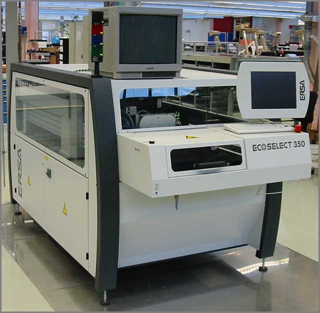 Image 5: Wave Soldering
4.2 Selective Wave Soldering Guidelines
When you buy a selective wave soldering machine, software and guidelines will come. Generally, you will need to do the following three steps to do the work:
You need to apply the liquid flux,
Assemble the PCB or preheating,
It would help if you soldered using a "site-specific" solder nozzle.
4.3 Selective Soldering problems
In selective soldering, you can encounter the following problems:
1. Copper pad dissolution: High temperature can dissolve the copper pad into the molten solder.
2. Solder balling: Solder balls can be formed due to sticking the solder mask at high temperatures.
3. Solder bridging: Excess solder can make an additional connection between two pins.
4. Solder Stringing: Solder remains across the solder nozzle can cause it.
4.4 Selective Wave Soldering Machine Cost
If you want to compare selective soldering machines with wave soldering machine costs, you will be pleased to know that selective soldering will be five times cheaper.
It will be because of less electricity requirement, less flux and solder consumption, no cleaning, less rework, and no protective taping.
Hopefully, you can now decide about the soldering technique that you want to use.
But before you make your final decision, we have also mentioned the defects, costs, and wave soldering problems in the next chapter.
5、Wave Soldering Defects and Problems
5.1 Wave Soldering Defects and Problems
If temperature and soldering environment are not adequately controlled, you will encounter the following defects after the wave soldering process:
Cavities
Cracks
Poor Conductivity
Inadequate solder thickness
And these are a few problems with wave soldering:
Higher consumption of electricity, flux, solder, and nitrogen
Need for solder rework
Extra sensitive points masking
Extra cleaning of soldered assemblies waves, solder aperture masks, or pallets.
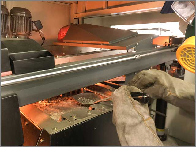 Image 6: Wave Soldering
5.2 Cost
So, now after reading the whole article, can you guess the operating costs of a wave solderings machine? You can imagine concerning selective soldering. Because of the abovementioned problems and defects, wave solderings can be five times more expensive.
6、Conclusion
In this guide, we have explained everything related to the waves soldering process. We have even mentioned the alternates of soldering methods.
We aimed to clear out any questions you may have regarding wave solderings. Now, you can easily decide which soldering suits you and when.
Moreover, you can contact us to manufacture PCB or enjoy its assembly. We will guide you in every possible way. You can even ask us about the techniques we use for PCB assembly.
And, if you have any questions, our team of experts and engineers will answer them at their earliest. We know how to take care of your interests and needs. Contact us at [email protected].
Special Offer: Get $100 off your order!
Email [email protected] to get started!


