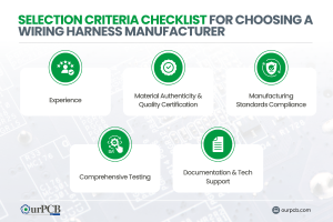
Top 10 Classic Car Wiring Harness Manufacturers | Full Guide
Finding the right wiring harness manufacturer for your vintage ride can be a real headache. Those beautiful old machines need special wiring that looks period-correct

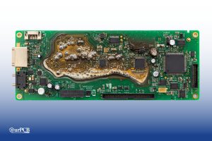
OurPCB, founded in 2007 in China, provides PCB fabrication, custom PCB design, and PCB assembly services. We ship directly from China to the USA and serve clients worldwide. With three facilities and dedicated account managers, we ensure reliable quality, fast turnaround, and cost-effective PCB solutions.


Feel free to check our capability overview below, and contact us if you have any special requirements not listed. As expert PCB board maker, we deliver high-quality PCB assembly services to meet your electronic needs.
| Specification | PCB Capability |
|---|---|
| Layer Counts | 1-64 layers |
| Lead Time | Normal: 5-6 Days Expedited: 24-48Hours |
| Materials | FR4, High TG FR4,Halogen Free material,CEM-3, Rogers HF material, etc. |
| Finished Copper Thickness | Up to 1000 μm |
| Finished Board Thickness | 0.1-12mm |
| Min. Line/Track Width&Space | 1.8/1.8 mil |
| Qualifications | ISO14001:2015, ISO9001:2015, ISO 13485:2016, IATF16949: 2016, Certified |
| Technology | On-Across Blindried Vias, Characteristic Impedance Control, Rigid-flex Board etc. |
| Solder Mask Color | green, black, blue, white, red, yellow, and matt, etc. |
| Legend/Silkscreen Color | white, yellow, black, etc. |
| Surface Treatment | HASL, Lead free HASL, ENIG(+ G/F), Immersion silver/Tin, OSP, ENEPIG, bare copper |
| Wrap and Twist | ≤0.5% |
| Other Technology | Gold finger, peelable mask, Non-across blind/buried vias, characteristic impedance control, Rigid-flex board etc. |


The choice of materials in PCB manufacturing affects the board’s performance and suitability for different applications:

A common fiberglass-reinforced epoxy laminate, known for its durability and electrical insulating properties.
Composite materials offering cost-effective alternatives for less demanding applications.
Such as polyimide, used for creating bendable and foldable PCBs.
Designed for applications requiring minimal signal loss and high-speed data transmission.
At OurPCB we offer PCB services for all PCB materials, layers and industries. Choose from our comprehensive list of services below.

Choosing the right PCB manufacturer is critical to ensuring quality and performance in your final product. Here’s why OurPCB stands out:

ISO 9001, UL, and RoHS certified manufacturing facilities ensuring compliance and safety.
Expertise in multilayer (up to 64 layers), HDI, and rigid-flex PCBs.
Competitive pricing for both low-volume prototypes and high-volume production orders.
Fast international delivery and responsive technical support available 24/7.
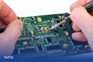
End-to-end service from design verification, sourcing components, to full assembly.
We handle everything from parts sourcing to final assembly, providing a hassle-free experience that ensures top-quality boards every time.
Whether you need a few prototypes or large-volume batches, our flexible assembly services adapt to your project’s scope and timeline.
Stay environmentally responsible with our compliant assembly processes, offering RoHS and lead-free options for safe, reliable builds.
No matter the complexity, we can assemble boards of all configurations—single-layer, multi-layer, or a mix—to match your exact specifications.
From one-off prototypes to bulk orders, we accommodate projects of all sizes without compromising on quality or turnaround time.
Join our growing community of satisfied clients who rely on our dependable assembly expertise and dedicated customer support.
Mon-Fri: 24 hours,
Sat: 9am-6pm, GMT+8
Reach us at
[email protected]
24 hours online
+86-199-30589219
Mon-Fri: 24 hours,
Sat: 9am-6pm, GMT+8
OurPCB offers cost-effective solutions for custom PCB manufacturing. The cost of producing a custom PCB depends on several factors:
At OurPCB, we follow stringent Understanding IPC Standards guidelines, alongside our ISO and UL certifications. We also help customers Explore PCB Components so they understand the role each part plays in overall quality.
At OurPCB, we are committed to minimizing the environmental impact of our PCB manufacturing process through responsible practices and sustainability initiatives:
At OurPCB, we utilize a range of advanced software tools to ensure precision and efficiency throughout the PCB manufacturing process:
At OurPCB, we adhere to a range of industry regulations and certifications to ensure that our PCBs meet the highest standards of safety, reliability, and quality:
Click here to download all of our Certifications.
PCB manufacturing is the process of creating Printed Circuit Boards (PCBs) that mechanically support and electrically connect electronic components using conductive tracks, pads, and other features.
Manufacturing times depend on the complexity and volume of the order. Standard lead time is 7-10 business days for small batches, but we offer expedited services for urgent projects.
We have no minimum order quantity, allowing you to order anything from single prototypes to mass production runs.
We offer a variety of articles and guides to help customers better understand PCB technology:
Absolutely. For hobbyists and engineers learning the basics, we feature tutorials like the 10 Minute Timer Circuit Design, which demonstrate principles before scaling up to commercial production.
Yes. In addition to OurPCB’s PCB Manufacturing Services, we are also trusted circuit card assembly providers offering full Electronics Manufacturing Services. This end-to-end approach ensures high-quality boards from design to delivery.
Finding the right wiring harness manufacturer for your vintage ride can be a real headache. Those beautiful old machines need special wiring that looks period-correct
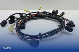
Would your car be able to run without wire harnesses? Not a chance. Wire harnesses connect all the electrical parts together. No harness means no
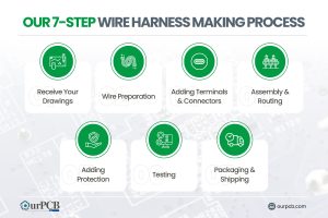
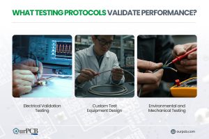
Making wire harnesses isn’t complicated. At OurPCB, we create custom wire harnesses for an expansive range of industries every day. While it’s a complicated process,
Prototype cable assemblies are the very important place in between PCB design ideas and interconnects. OurPCB brings prototype assemblies with PCB solutions to your tables.
PCB thermal management prevents component overheating through strategic heat transfer techniques. Without proper thermal control, electronics are at risk of electronic failures through weakened solder
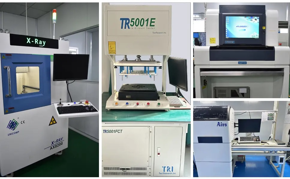
ContentsKey TakeawaysWhat is a Multilayer-Printed Circuit Board?How do Multilayer PCB Boards Work?Multilayer PCB ApplicationsMultilayer PCB Manufacturing Process: StepsMultilayer PCB Manufacturing MachinesBenefits of Multilayer Circuit BoardsWhat
We use cookies to improve your browsing experience, which may include personal information. By clicking "Agree," you accept our Privacy Policy and cookie use. You can change your cookie settings in your browser anytime.
Agree
 Chat With Us
 Free Quote