Contents
- General PCB Design Best Practices
- 1. Avoid Common Mistakes
- 2. Follow Industry Guidelines
- 3. Prioritize Functionality over Aesthetics
- Layout Optimization Techniques
- 4. Strategize Component Placement
- 5. Optimize Trace Routing
- 6. Design Multilayer PCBs Carefully
- Signal Integrity Considerations
- 7. Mitigate Electromagnetic Interference (EMI)
- 8. Design for High-Speed Signals
- 9. Manage Ground Planes and Loops
- Power Distribution and Thermal Management
- 10. Optimize Power Delivery Network (PDN)
- 11. Manage Heat Dissipation
- PCB Design Software and Tools
- 12. Choose the Right Design Software
- 13. Leverage Design Automation Features
- Design for Manufacturability (DFM)
- 14. Ensure Production-Ready Designs
- 15. Validate Designs Through Testing
- Specialized PCB Design Considerations
- 16. Design for IoT Applications
- 17. High-Frequency PCB Design
- 18. Ruggedized PCB Design
General PCB Design Best Practices
Let's start with some fundamental principles that form the foundation of good PCB design, essential for any PCB design company aiming to create high-quality products.
1. Avoid Common Mistakes
One of the first steps in creating a reliable PCB layout is to be aware of and avoid common pitfalls. Here are some key areas to focus on:
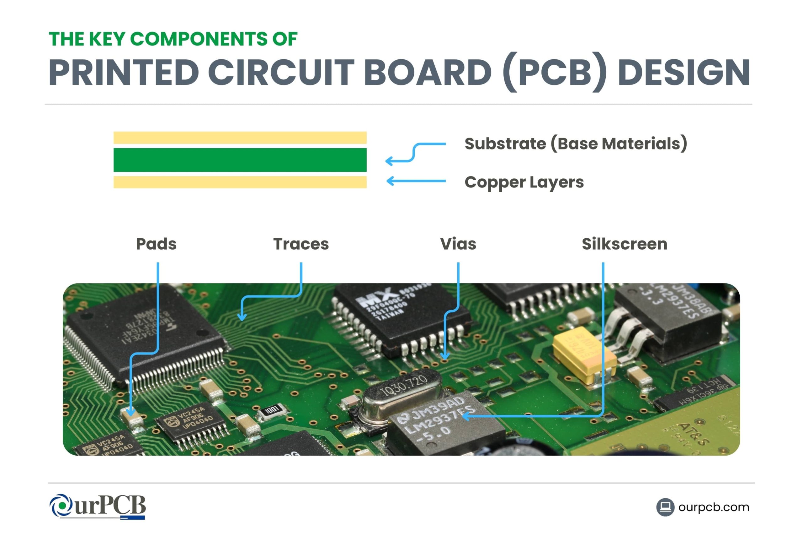
- Component footprints: Ensure that the footprints in your design match the actual physical components you'll be using. Mismatched footprints can lead to assembly issues or even render the board unusable.
- Component spacing: Provide adequate clearance between components to facilitate soldering and prevent interference. This is especially important for hand-soldered boards or when using automated assembly equipment. Understanding potential assembly challenges, as discussed in common LED PCB assembly issues, can help you avoid errors during production.
- Part selection and orientation: Double-check that you've selected the correct parts and oriented them properly in your design. Incorrect orientation can lead to non-functional circuits or damaged components.
- Small component management: Pay special attention to small components that can be challenging to place and solder. Consider using larger package sizes for passive components if space allows, to improve manufacturability.
- VIA placement: Verify that vias are not placed too close to pads, as this can cause potential shorts during the manufacturing process. Follow your fabricator's design rules for minimum via-to-pad spacing.
2. Follow Industry Guidelines
To ensure your PCB designs meet professional standards, it's crucial to understand and adhere to industry guidelines:
- Basic PCB design principles: Familiarize yourself with fundamental concepts such as controlled impedance, signal integrity, and power distribution. Resources like “High-Speed Digital Design“ by Howard Johnson and Martin Graham can provide valuable theoretical background.
- Technical terminology: Learn and use proper technical terms and industry jargon. This will help you communicate effectively with manufacturers and other professionals in the field.
- IPC standards: Refer to standards like IPC-2221 for generic PCB design requirements. These guidelines cover various aspects of PCB design, including material selection, conductor spacing, and hole sizes.
- SMD land pattern guidelines: Consult resources like IPC-7351 for surface-mount device (SMD) land pattern recommendations. These guidelines ensure proper component attachment and solder joint reliability.
3. Prioritize Functionality over Aesthetics
While a visually appealing PCB layout can be satisfying, it's essential to focus on functionality first:
- Circuit performance: Ensure that your layout optimizes the circuit's electrical performance. This includes minimizing noise, maintaining signal integrity, and providing adequate power distribution.
- Signal integrity: Pay close attention to critical signal paths, keeping them short and direct to minimize interference and maintain signal quality.
- Power distribution: Design your power planes and traces to provide clean, stable power to all components on the board.
- Thermal management: Consider the thermal requirements of your components and design the layout to facilitate proper heat dissipation. Collaborating with a reliable metal core PCB manufacturer can help ensure that your PCB incorporates advanced thermal management techniques, enabling it to handle high-power applications effectively.
Once you've addressed these functional aspects, you can then focus on improving the appearance and manufacturability of your design.
Layout Optimization Techniques
Now that we've covered the general best practices, let's delve into specific techniques for optimizing your PCB layout.
4. Strategize Component Placement
Effective component placement is crucial for creating a reliable and efficient PCB layout. Consider the following strategies:
- Start with key components: Begin by placing connectors, test points, and edge-mounted components. These often have fixed positions due to mechanical constraints or user interface requirements.
- Group related components: Place highly interconnected parts close together to minimize trace lengths. This can improve signal integrity and reduce electromagnetic interference (EMI).
- Space out high-pin-count ICs: Allow sufficient space around complex integrated circuits to facilitate easier routing between their pins.
- Optimize decoupling capacitor placement: Position decoupling capacitors as close as possible to the power pins of the ICs they serve. This minimizes the loop area and improves their effectiveness in reducing power supply noise.
5. Optimize Trace Routing
Proper trace routing is essential for maintaining signal integrity and minimizing interference. Follow these best practices:
- Layer stack-up considerations: Route critical high-speed signals on inner layers between solid ground planes. This provides better shielding and controlled impedance.
- Keep traces short and direct: Minimize trace lengths, especially for high-speed or sensitive signals, to reduce noise and maintain signal integrity. For additional strategies to address signal-related challenges, consider these tips for controlling impedance.
- Avoid right-angle bends: Use 45-degree angles or curved traces instead of right-angle bends. This helps prevent impedance discontinuities and reduces electromagnetic emissions.
- Maintain consistent trace widths: For controlled impedance traces, ensure that the width remains consistent throughout the route. Changes in width can cause reflections and signal degradation.
6. Design Multilayer PCBs Carefully
When working with multilayer PCBs, consider these additional layout techniques:
- Adjacent power and ground planes: Place power and ground planes adjacent to signal layers for better isolation and reduced crosstalk.
- Tight coupling: Ensure tight coupling between signal layers and their reference planes to maintain consistent impedance and reduce EMI.
- Judicious via usage: Use vias carefully, avoiding thermal relief vias unless absolutely necessary. Excessive use of vias can introduce discontinuities and affect signal integrity.
- Orthogonal routing: Route high-speed signals orthogonally (at right angles) between layers to reduce crosstalk between parallel traces on adjacent layers.
Signal Integrity Considerations
Maintaining signal integrity is crucial for ensuring reliable operation of your PCB, especially in high-speed circuits or sensitive designs. Let's explore some key considerations.
7. Mitigate Electromagnetic Interference (EMI)
EMI can cause significant issues in PCB performance. Implement these techniques to minimize its impact:
- Proper grounding and shielding: Use a solid ground plane and consider adding shield traces or planes around sensitive signals.
- Controlled impedance: Maintain consistent impedance for high-speed signal traces to prevent reflections and signal degradation.
- Strategic decoupling: Use decoupling capacitors to filter power supply noise effectively. Place them close to ICs and use a variety of capacitor values to cover a wide frequency range.
- Avoid unintentional antennas: Minimize long, unshielded traces that can act as antennas and radiate or pick up EMI. For more effective approaches to EMI reduction, explore these guidelines for EMI mitigation.
8. Design for High-Speed Signals
High-speed signals require special attention to maintain their integrity:
- Minimize trace lengths: Keep high-speed signal traces as short as possible to reduce the potential for interference and signal degradation.
- Match differential pairs: For differential signals, ensure that the pair of traces are matched in length and routed close together to maintain common-mode rejection.
- Use appropriate transmission line structures: Utilize microstrip or stripline topologies to maintain consistent impedance for high-speed signals. For more information on best practices, check out these helpful guidelines for high-speed PCB design.
- Implement proper termination: Add termination resistors to minimize reflections on high-speed lines. The specific termination method (series, parallel, or differential) will depend on your circuit requirements.
9. Manage Ground Planes and Loops
Proper ground management is crucial for maintaining signal integrity and reducing EMI:
- Continuous ground plane: Maintain a continuous, uninterrupted ground plane on the bottom layer of your PCB. This provides a low-impedance return path for signals and helps reduce EMI.
- Avoid splits and cuts: Refrain from splitting or cutting the ground plane, as this can create discontinuities and noise issues.
- Use stitching vias: Implement stitching vias to connect ground planes between layers, ensuring a low-impedance path for return currents.
- Minimize loop areas: Keep the area of power and signal return current loops as small as possible to reduce EMI and improve signal integrity.
Special Offer: Get $100 off your order!
Email [email protected] to get started!
Power Distribution and Thermal Management
Proper power distribution and thermal management are critical for ensuring reliable operation of your PCB. Let's explore some best practices in these areas.
10. Optimize Power Delivery Network (PDN)
An effective PDN ensures that all components receive clean, stable power:
- Adequate trace widths: Route power traces with sufficient width to handle the required current without excessive voltage drop or heating.
- Strategic decoupling: Place decoupling capacitors close to the power pins of ICs they serve. Use a combination of capacitor values to provide effective decoupling across a wide frequency range.
- Multiple power/ground plane pairs: For complex designs, consider using multiple power and ground plane pairs to provide low-impedance power distribution.
- Isolation jumpers: Consider adding isolation jumpers to separate different sections of the PDN. This can help isolate noise-sensitive circuits from noisy power domains.
11. Manage Heat Dissipation
Effective thermal management is crucial for preventing component failures and ensuring long-term reliability:
- Thermal vias: Incorporate thermal vias under high-power components to improve heat transfer to other layers or a heatsink on the opposite side of the board.
- Heatsinks and airflow: For components generating significant heat, consider using heatsinks and plan for adequate airflow in your enclosure design.
- Component placement: Avoid placing heat-sensitive parts near heat-generating components. Consider the overall thermal distribution across your board.
- Thermal simulation: Use thermal simulation tools to identify and address potential hot spots in your design before manufacturing.
PCB Design Software and Tools
Choosing the right design software and leveraging its features can significantly improve your PCB design process.
12. Choose the Right Design Software
Selecting appropriate PCB design software is crucial for efficient and accurate design:
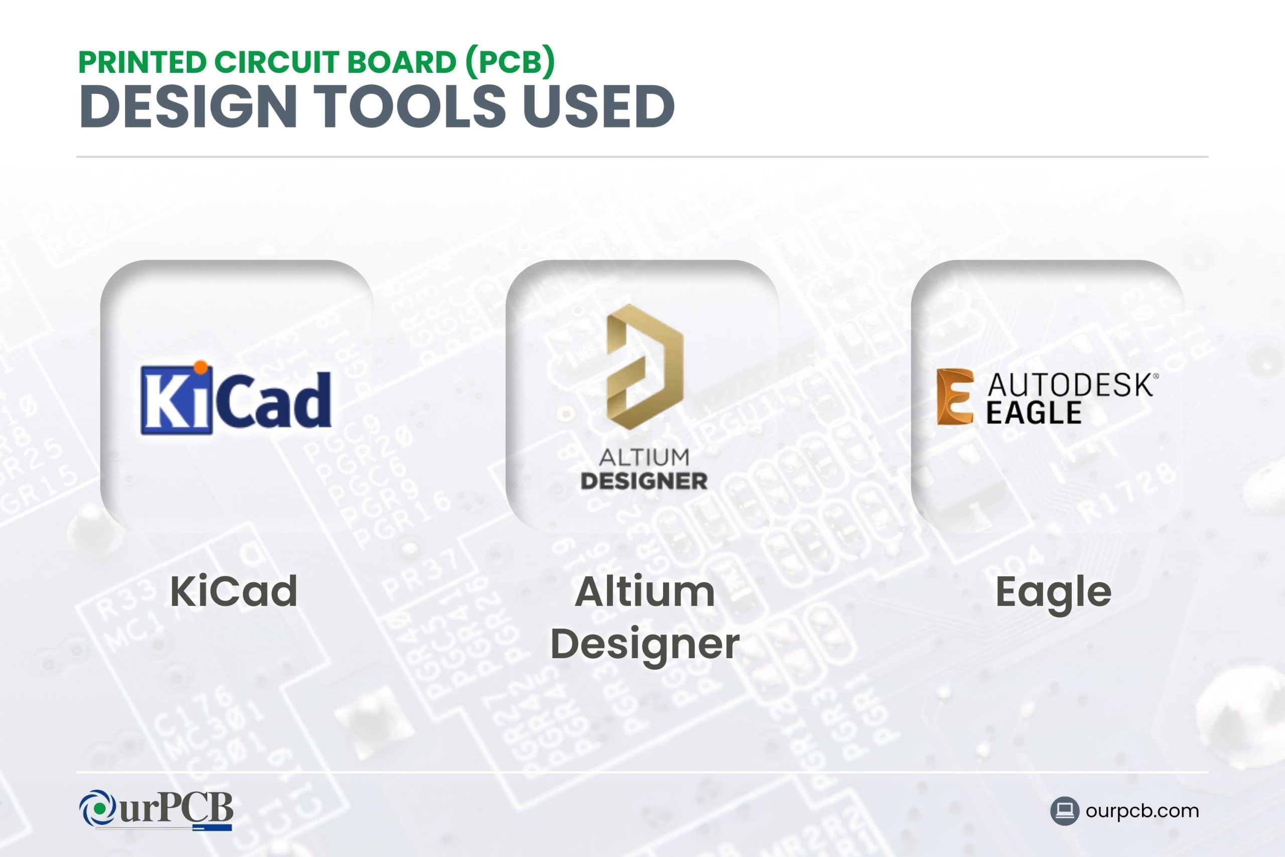
- Open-source options: For hobbyist projects or those on a tight budget, consider open-source tools like KiCad or Eagle (free version).
- Professional-grade tools: For complex designs or professional use, invest in tools like Altium Designer, OrCAD, or Cadence Allegro.
- Feature evaluation: Ensure the software supports the features you need, such as 3D visualization, signal integrity analysis, or integration with mechanical CAD tools.
- Proficiency: Invest time in learning your chosen PCB design tool thoroughly. Many offer tutorials, documentation, and user communities to help you become proficient.
13. Leverage Design Automation Features
Modern PCB design software offers various automation features to improve efficiency and reduce errors:
- Design Rule Checking (DRC): Utilize built-in DRC tools to validate your layout against manufacturing constraints and best practices.
- Autorouting: While not perfect, autorouting can be useful for non-critical traces. Always review and optimize autorouted results manually.
- Simulation tools: Explore integrated or third-party simulation tools for signal integrity, power integrity, and thermal analysis to validate your design before manufacturing.
- Custom scripts and macros: Learn to use scripting capabilities in your design software to automate repetitive tasks and improve productivity.
Design for Manufacturability (DFM)
Ensuring your PCB design is optimized for pcb manufacture is crucial for reducing costs and improving yield.

14. Ensure Production-Ready Designs
Follow these guidelines to create designs that are ready for manufacturing:
- Optimize for manufacturing: Consider factors like component placement and trace routing that affect the ease of manufacturing and assembly.
- Adhere to fabricator guidelines: Follow the design rules and constraints provided by your PCB fabricator. This includes minimum trace widths, spacing, and via sizes.
- Perform DFM checks: Use DFM checking tools to identify potential manufacturing issues before sending your design for production.
- Collaborate with manufacturers: Maintain open communication with your PCB manufacturer throughout the design process. They can provide valuable insights and recommendations.
15. Validate Designs Through Testing
Thorough testing is essential to ensure your PCB design functions as intended:
- Incorporate test features: Add test points and debug headers to aid in board bring-up and troubleshooting.
- Use simulation tools: Leverage circuit simulation tools to verify performance and identify potential issues before manufacturing.
- Conduct thorough testing: Perform comprehensive functional and environmental testing on prototype boards before moving to full production.
- Document the process: Maintain detailed records of your design process, including decisions made and issues encountered, for future reference.
Specialized PCB Design Considerations
Different applications may require specific design considerations. Let's explore some specialized areas of PCB design.
16. Design for IoT Applications
Internet of Things (IoT) devices often have unique requirements:
- Communication protocols: Select appropriate wireless protocols (e.g., LoRaWAN, Bluetooth, Wi-Fi) based on your application's range, power, and bandwidth needs.
- Power optimization: For battery-powered devices, optimize your design for low power consumption. Consider using low-power components and implementing sleep modes.
- Antenna design: Ensure reliable wireless connectivity by carefully designing and placing antennas. Consider using pre-certified modules for complex RF designs.
- Environmental factors: Design for the intended operating environment, considering factors like temperature, humidity, and vibration.
17. High-Frequency PCB Design
High-frequency designs require special attention to maintain signal integrity:
- Controlled impedance: Maintain precise control over trace impedance for RF and microwave signals. This often requires close collaboration with your PCB manufacturer.
- Transmission line structures: Utilize appropriate microstrip or stripline topologies for high-frequency signals, ensuring consistent impedance throughout the signal path.
- Minimize discontinuities: Carefully design transitions between different transmission line structures to minimize reflections and signal loss.
- Isolation techniques: Implement proper shielding and isolation techniques to prevent crosstalk between high-frequency signals and other parts of your circuit.
18. Ruggedized PCB Design
For PCBs intended for harsh environments, consider these design aspects:
- Component and material selection: Choose components and PCB materials rated for the intended operating conditions (temperature range, humidity, etc.).
- Protective measures: Implement conformal coatings or potting compounds to protect against moisture, dust, and chemical exposure. Design appropriate enclosures for additional protection.
- Mechanical integrity: Ensure reliable interconnections by using appropriate connector types and considering strain relief for cables. Use adequate mounting holes and consider the effects of vibration on your design.
- Extensive testing: Conduct thorough environmental and stress testing to validate the design's durability under expected operating conditions.
Back to top: PCB Design and Layout Tips and Best Practices
Special Offer: Get $100 off your order!
Email [email protected] to get started!