Contents
- Why is Copper Used in PCB?
- Types of Copper Used in PCBs
- Design Considerations
- Calculating Copper Thickness for PCB Traces
- Impact of Copper Weight on PCB Performance
- Copper Layer Guidelines in Multi-layer PCBs
- Manufacturing Processes
- Common Issues and Solutions with Copper in Printed Circuit Boards
- Copper Trace Defects and Troubleshooting
- Fixing Copper Peeling During Manufacturing
- How to Choose Copper Thickness on a PCB
Why is Copper Used in PCB?
The combination of copper's excellent electrical conductivity, current-carrying capacity, thermal management properties, and manufacturability make it the preferred choice as the primary conductive material in printed circuit boards.
Key Reasons Why Copper Is Used in PCBs:
Electrical Conductivity
- Copper has a low electrical resistivity of 1.68 μΩ-cm, making it an excellent conductor for PCB applications.
- Its high electrical conductivity, around 5.96 × 10^7 Siemens per meter, allows for efficient signal transmission and power distribution on PCBs.
Current-Carrying Capacity
- Thicker copper layers (e.g., 2 oz or 3 oz) can carry higher currents before reaching critical temperature rises compared to thinner 1 oz copper traces.
- The current-carrying capacity of copper traces is crucial for PCB designs that require high-power or high-current handling.
Thermal Management
- Copper layers and traces act as heat spreaders, dissipating heat generated by high-power components on the PCB.
- The thermal conductivity of copper helps transfer heat away from critical components, improving overall thermal management.
Manufacturability
- Copper is the primary material used for conductive layers in PCBs because it can be easily etched, plated, and deposited during the manufacturing process.
- Various copper foil types, such as electrodeposited and rolled-annealed copper, offer flexibility in PCB fabrication.
Cost-Effectiveness
- Copper is relatively inexpensive and widely available, making it a cost-effective choice for PCB manufacturing compared to other conductive materials like silver or gold.
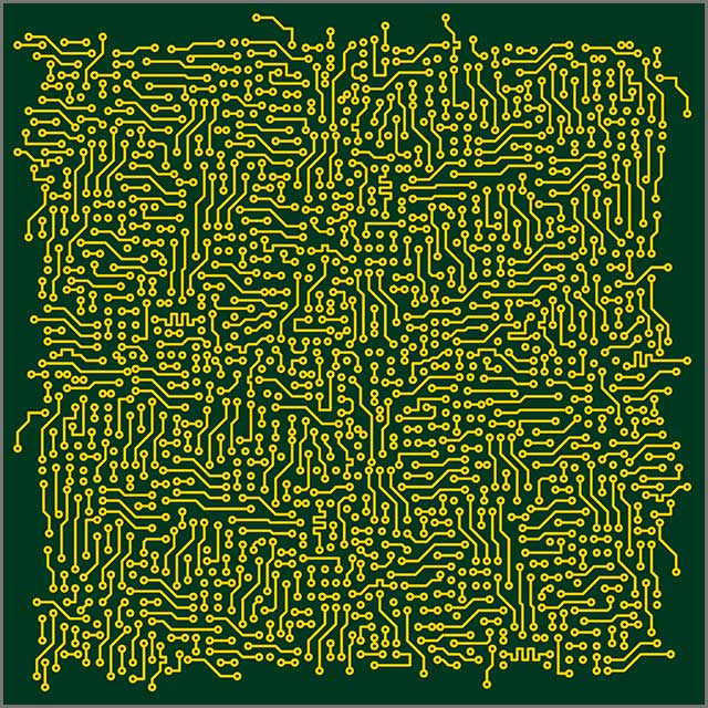 Image 1: Copper PCB
Special Offer: Get $100 off your order!
Email [email protected] to get started!
Types of Copper Used in PCBs
Copper Foils
- PCBs are commonly constructed using copper foils laminated onto a dielectric substrate. Typical copper foil thicknesses include 0.5 oz, 1 oz, 2 oz, and 3 oz per square foot.
Electrodeposited Copper
- This type of copper is applied to the PCB surface through an electroplating process and is often used to form copper barrels in vias and other drilled holes.
Rolled-Annealed Copper
- Produced through rolling and annealing, this copper is mechanically stronger and more robust than electrodeposited copper, making it suitable for certain applications.
Design Considerations
Calculating Copper Thickness for PCB Traces
The thickness of copper on a PCB trace is typically measured in ounces per square foot (oz/ft²) or micrometers (μm). 1 oz of copper per square foot corresponds to a thickness of approximately 1.34 mils (34 μm). The resistance of a PCB trace is inversely proportional to its cross-sectional area, which is determined by the trace width and thickness.
Impact of Copper Weight on PCB Performance
Thicker copper layers (e.g., 2 oz or 3 oz) can provide lower electrical resistance, higher current-carrying capacity, and improved thermal dissipation compared to standard 1 oz copper. However, using thicker copper also increases the cost of the PCB, so the benefits must be weighed against the additional expense.
Copper Layer Guidelines in Multi-layer PCBs
In a multi-layer PCB, the copper layers can be used for signal routing, power distribution, and ground planes. It is recommended to balance the copper distribution across the layers to prevent warping and maintain symmetry in the PCB construction. Typical copper layer configurations include 4-layer (2 signal, 2 power/ground), 6-layer (4 signal, 2 power/ground), and 8-layer (6 signal, 2 power/ground) designs.
Manufacturing Processes
Copper Etching on PCBs
- The copper layers on a PCB are patterned through an etching process, where unwanted copper is removed to create the desired circuit traces and features.
- Variations in trace width and thickness during etching can affect the electrical and thermal performance of the PCB.
Copper Plating Techniques
- Electroplating is a common method for depositing copper onto the PCB surface, especially for forming copper barrels in vias and other drilled holes.
- Electroless plating, which does not require an electrical current, is often used for applying protective coatings on exposed copper surfaces.
- Advanced techniques like reverse pulse plating (RPP) enhance the ability to plate copper in small, high-aspect-ratio holes.
Copper Thieving
- Copper thieving involves adding small, isolated copper pads to the PCB surface to balance copper plating distribution and ensure uniform copper thickness across the board.
Common Issues and Solutions with Copper in Printed Circuit Boards
Copper Trace Defects and Troubleshooting
Copper traces on PCBs can be susceptible to various issues, such as shorts, opens, and delamination, which can be caused by manufacturing defects, design flaws, or environmental factors. Effective troubleshooting and quality control measures are crucial to identify and address these copper-related problems during the PCB fabrication process.
Fixing Copper Peeling During Manufacturing
Copper peeling, where the copper layer delaminates from the PCB substrate, can be a common issue during the manufacturing process. Proper surface preparation, adhesion enhancement techniques, and careful control of the lamination and etching processes can help mitigate copper peeling problems.
How to Choose Copper Thickness on a PCB
The thickness of a PCB will vary based on the number of copper layers used. Nonetheless, thicker boards work best because thinner ones are prone to breaking.
The cost increases when you opt for a thicker copper layer, but this can be crucial in some instances.
For instance, when you have determined that your electronic device's design will need a more significant current than what a typical PCB can hold.

Special Offer: Get $100 off your order!
Email [email protected] to get started!


