A printed circuit board (PCB) provides the platform to physically and electronically link electronic components. You can think of it as the base upon which you build up any electronic device.
At the heart of the PCB board is a layer or multiple layers of copper lined vertically to the board’s plane. These films make up PCB layers.
Contents
- What are PCB Layers?
- Core Layers
- External Layers
- What are the Types of PCB Layers?
- Conductive Layer
- Insulation Layer
- Solder Mask Layers
- Silkscreen Layers
- Internal Split Planes
- Thieving Planes (or Copper Thieves)
- What is PCB Layer Stackup?
- Common Configurations of PCB Layers
- Single-Layer PCBs
- Double-Layer PCBs
- Multilayer PCBs
- What is the PCB Manufacturing Process for Layers?
- Step-by-Step Guide to PCB Manufacturing for Layers
- What are Flexible and Rigid-Flex PCBs?
- What Materials are Used in PCBs?
- Substrates
- Conductive Materials
- Insulating Materials
- PCB Layers FAQs
- What is the Difference Between 4-Layer and 6-Layer PCB?
- How Many Layers can a PCB Have?
- How are PCB Layers Held Together?
- Final Thoughts
What are PCB Layers?
A PCB layer is a film of copper with signal transmitting capacity lined up vertically to the board's plane. There are numerous types of PCB boards, and they derive their name from the number of layers present.
For example, when a board features only the top and the bottom layers, we refer to it as a two-layered board. Similarly, a board comprising a top layer, a bottom layer, and three inner layers in the middle is a five-layered board. Also noteworthy is that PCB layers have a Fire Retardant Version4 (FR4) insulating substrate separating one from the other.
Core Layers
The core layers in PCBs are of three primary types:
- Signal Layers: As per its name, this is the layer where the electrical signal transmission occurs. It’s where you’ll connect parts such as the ICs, capacitors, resistors, and others that enable current flow.
- Power Planes: A power plane is also a core PCB layer that provides a viable low-impedance electrical path for current flow to PCB parts. The power plane is usually extensive by design to facilitate seamless voltage flow. Also, owing to its role in streamlining the signal flow, the power plane is a common feature in high-current circuitry.
You’re also likely to find it in other systems where a stable power supply is cardinal.
- Ground Plane: A ground plane resembles a power plane, but this one caters for the return signal. The ground plane connects to the ground as per its name. It’s essential, especially in curtailing electromagnetic interference's effect, ensuring signal integrity maintenance.
External Layers
The layers described above form the heart of any PCB, but there are two essential layers lacing the top and the bottom of the printed circuit board. We refer to these as the PCB’s top and bottom layers.
In principle, they’re similar to the typical signal layers but provide a platform for housing the PCB’s other components. Besides giving a base for routing signals, you attach capacitors, resistors, ICs, etc., to these layers.
What are the Types of PCB Layers?
PCB layers come in various types: conductive, insulation, solder mask, silkscreen, internal split planes, and thieving planes. Let's explore the individual types of layers and their characteristics in detail.
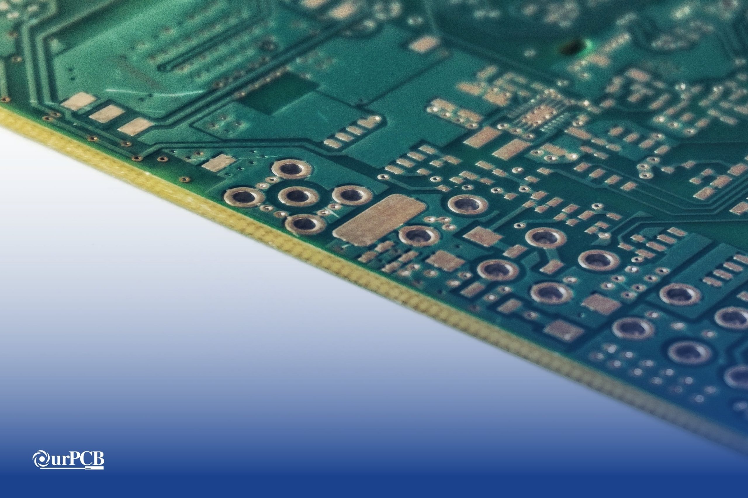
Conductive Layer
This is arguably the most important layer in any PCB type, as it facilitates the transmission of signals across the components. It’s typically copper-made owing to the material’s excellent conductivity features.
The variations in the copper quality are responsible for determining its overall quality. If the copper is of substantive thickness, it has great conducting capacity, and the PCB also has excellent functionality.
Insulation Layer
The conductive layers need a separation material to prevent interference when conducting. This material must have excellent electrical insulation properties and is placed between the conductive layers.
Therefore, all PCBs will feature a dielectric insulation material, usually of the frame retardant (FR-4) grade. Some common insulators include epoxy resin, ceramic substrates, and polyimide. Fiberglass is also popular with most PCBs thanks to its excellent insulation features.
Solder Mask Layers
When observing the most common PCBs, it’s easy to see the green coloring covering the top and bottom parts. This is the solder mask layer, which is cardinal in enhancing the PCB’s functionality. It plays a crucial role in preventing shorting, which can happen when dust accumulates on the PCB.
Despite its apparent significance on the PCB, it’s not on all circuit boards. In some boards, you’ll find it only on a single side, so it all depends on the overall PCB design. However, its presence is a big plus because it also discourages the oxidation of the conducting surface in PCBs.
Silkscreen Layers
A PCB usually features inscriptions such as logos, printing labels, and the component values that guide you through its circuitry. This is the silkscreen layer, which plays a significant role during the components' mounting phase.
The inscriptions make it easy to troubleshoot PCBs and simplify assembly of the components.
Internal Split Planes
Power and ground planes carry opposite signal types. As the power plane carries a positive signal, the ground plane will have a negative one, and the internal split planes will be useful in enabling this separation.
In addition, the internal split planes facilitate digital and analog ground zones, which is essential in curtailing noise coupling. However, for the optimal effectiveness of these planes, it’s necessary to have well-placed segmentation lines at the PCB assembly phase.
This is especially important for complex circuits in small form factor devices where different voltage separations can be daunting.
Thieving Planes (or Copper Thieves)
Another thing you may have noted in PCBs is the square or round patches of copper on the board’s surface. This is a thieving plane, and it’s not connected to the primary circuit. Therefore, it doesn't affect the signal transmission processes.
Rather, thieving is essential to enhancing the integrity of the PCB. This is usually achieved by establishing an even distribution of copper over the PCBs, which is critical during the etching process.
What is PCB Layer Stackup?
PCB stack-up is how the circuit board’s layers are arranged to give the final PCB layout. As per its name, it defines the stacking up of the numerous PCB layers, which is imperative in combining different circuits into a single board. Other upsides of PCB layer stack-up include:
- It curtails a PCB's vulnerability to external noise/radiation exposure while lowering the chances of cross-talk and impedance.
- It’s essential for lowering PCB manufacturing costs as it combines different circuits in one board while maintaining signal integrity.
- An excellent PCB layer stack-up design is essential for keeping the circuit board free of electromagnetic interference.
There are numerous PCB layer stack-up configurations depending on the customer demands and the circuit board’s applications. Below is an example of a PCB layer stack-up for an eight-layer PCB design. Note that the layers are stacked up in the order illustrated below.
| Top Surface Layer | Solder Mask |
| Top Layer | High-Speed Signal Layer |
| Prepreg | |
| Layer Two | Ground Plane |
| Prepreg | |
| Layer Three | High-Speed Signal Layer |
| Core | |
| Layer Four | Ground Plane |
| Prepreg | |
| Layer Five | Ground Plane |
| Core | |
| Layer Six | High-Speed Signal Layer |
| Prepreg | |
| Layer Seven | Ground Plane |
| Prepreg | |
| Bottom Layer | High-Speed Signal Layer |
| Bottom Surface | Solder Mask |
You must exercise minimum space tracing, especially when comping the above stack into a small device. Also noteworthy in the above example is that parts of the stack include a prepreg or a core. Prepreg is a reinforcing material featuring a resin, while the core is usually a copper-plated glass-reinforced epoxy laminate.
The thickness of the core will vary depending on the form factor, but on average, it’s between 0.1mm to 0.3mm.
Special Offer: Get $100 off your order!
Email [email protected] to get started!
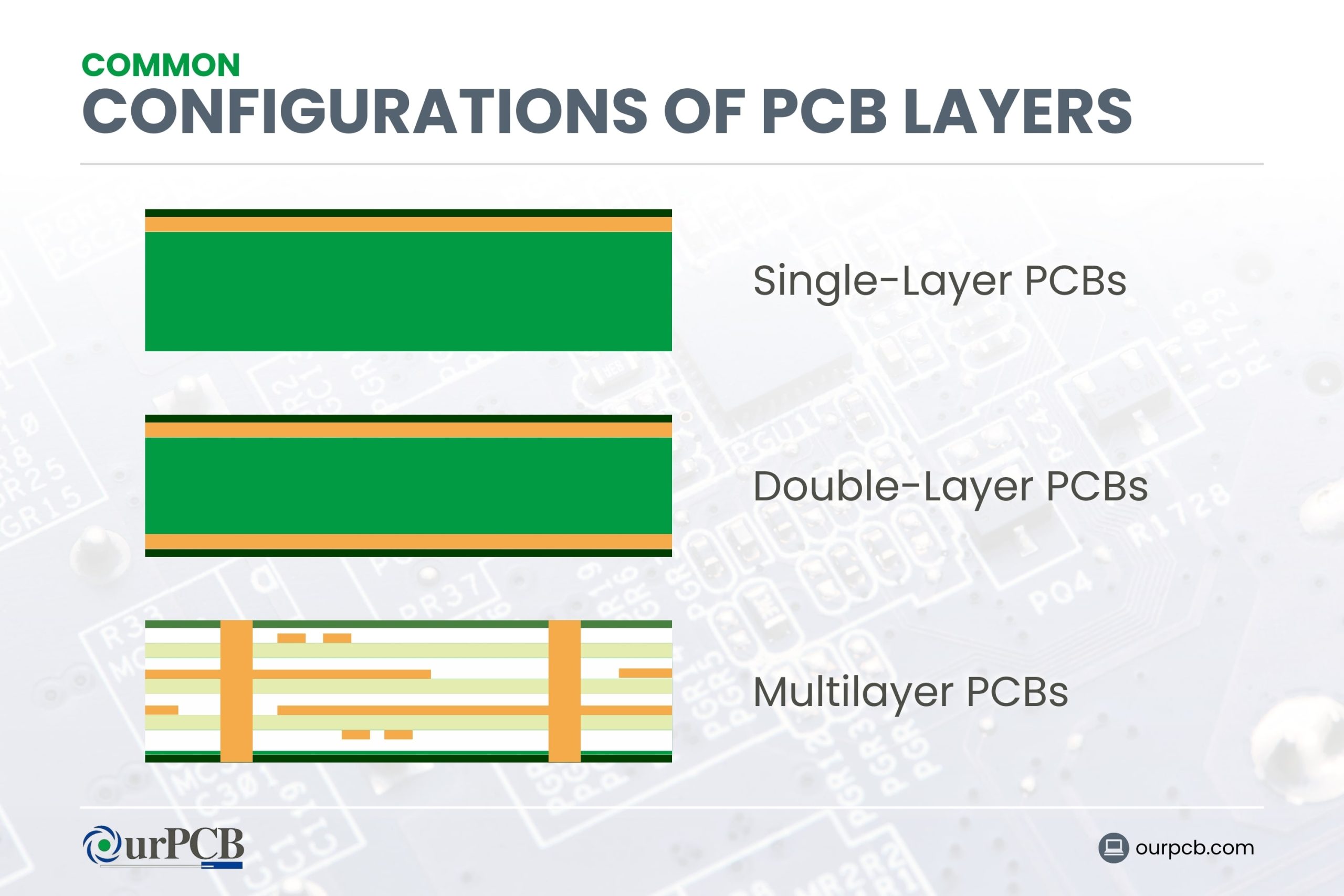
Common Configurations of PCB Layers
When you stack up a PCB, as illustrated in the example, you develop an eight-layer PCB configuration. There are many others, but the main ones are categorized into the following groups:
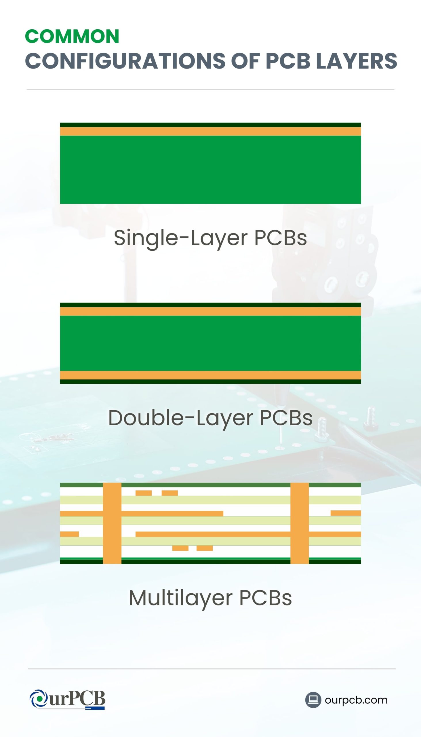
Single-Layer PCBs
This is a PCB comprising a single conducting (copper) layer. The reverse side of this PCB is where you attach the surface mount components.
Single-layer PCBs consist of four main parts:
- A conductive layer (copper layer) which forms the current pathway in the circuit board’s circuit.
- A substrate layer, which is usually made of a material such as FR-4 fiberglass.
- A silkscreen, which is handy in the mounting of components on the PCB by ensuring that there are visible inscriptions on the board.
- A solder mask, to offer protection to the single-sided PCB and ensure that dust accumulating on the PCB doesn’t lead to a shortcircuit.
Other parts of this PCB include pads and vias. The single-sided PCB is the simplest of PCBs and is crucial in simple electronics such as calculators and toys. Its simple structure also means that it’s cheap, and consequently, the appliances that use it are also inexpensive. Other upsides of the PCB include:
- It’s easy to manufacture and allows bulk production.
- Working with single-sided PCBs is a breeze due to its thin profile. You can easily make holes in it, while component mounting and soldering are also straightforward.
- There’s little chance for error during manufacturing owing to its simple design.
But while it’s undoubtedly an excellent option for simple DIY projects, the single-layer PCB has limitations:
- It has a relatively lower speed than other sophisticated PCB configurations. Its operation capacity is therefore limited to simple electronics such as toys.
- The PCB cannot also accommodate numerous components.
- The components on the PCB are prone to noise and electromagnetic interference.
- Modifying it to hold numerous parts will result in a relatively large size. This makes it unsuitable for use in devices with confined spaces, like smartphones.
Double-Layer PCBs
Also called a 2-sided PCB, this is a variation of the single-sided PCB, known for its capacity to hold components on either side of the PCB. It features two copper layers separated by a dielectric substrate layer lined up between them. The dielectric layer is essential in shielding the signals from either of the copper layers from interacting with each other.
A double-layer PCB’s structure allows for stacking a substantive number of components, more than a single-layer PCB. Nonetheless, you still cannot stack up numerous components in high-speed circuitry. Also noteworthy about the PCB is that it features vias perforated on the core, running from the top to the bottom layers. These are handy in connecting the traces from either side, although they take up substantive space.
Examples of the via types include through holes and blind and buried types, essential in enabling complex routing. So what are the upsides of this PCB type over the single-layer types?
- They allow a more dense circuitry and facilitate circuit flexibility.
- They’re more efficient in signal noise management thanks to the separating substrate layer.
Due to these properties, they’re suited to complex PCB applications such as HVAC systems, vending machines, and amplifiers.
Multilayer PCBs
These PCBs have more than two conductive (copper) layers separated by insulation (prepreg) layers. They undergo intense heat and pressure for a solid bond. These manufacturing conditions prevent air accumulation between the layers. If present, the air can affect the PCB’s reliability during use and also impact its performance.
There’s a burgeoning demand for small-form-factor electronic products. A single PCB with numerous layers would be vital to meeting this demand.
The insulating material is usually fibreglass-reinforced epoxy, and its primary function is to prevent electrical shorts between the layers. Other commonly used materials include Teflon and sophisticated ceramic.
Like the double-layer PCBs, these also feature a vias network running from the top to the bottom of the circuit boards. These are very important in enhancing intricate signal routing across the layers. In addition, these PCBs become more complex as the configuration of the number of layers grows.
The multilayer PCBs have dedicated power and ground planes to enhance their stability during use. It also has a single connection point unlike multiple single layers PCBS, which have multiple ones. Moreover it has a reduced form factor enabling reduction of board size to fit small spaces while having more functionalities.
Below are other features.
- They’re lightweight ensuring they’re fit for use in wearables such as smart watches.
- Capacity for use over an extended duration and ability to be remodeled for use in different applications.
- A network of internal layers that ensure excellent routing without the risk of electromagnetic interference.
So, what are their primary upsides?
- They perfectly fit PCBs for complex projects as they have more connection points and allow multiple circuits.
- A multilayer circuit board is relatively thicker than the single-layer and the double-layer type. This feature makes the multilayer PCB more durable and thus can exist in extreme work environments without the risk of breakdown.
- They’re the ideal PCBs for power-intensive devices as their structure enhances power distribution. There’s also a limited risk of electromagnetic interference with the signal integrity.
What is the PCB Manufacturing Process for Layers?
Layer construction is a critical process in PCB manufacturing and assembly. The layers are responsible for carrying current and providing power to the attached components. Below is a detailed elaboration of the process.
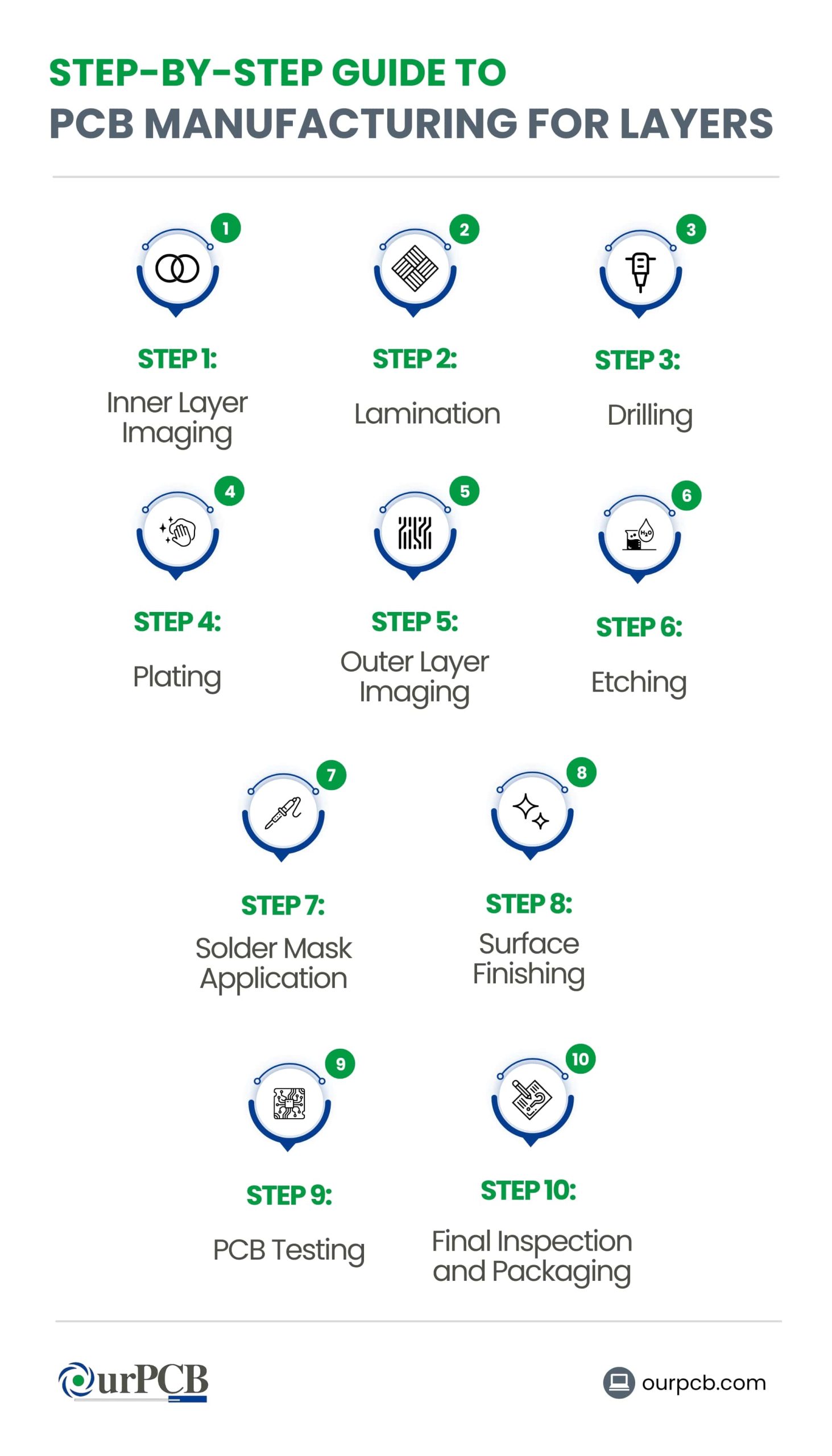
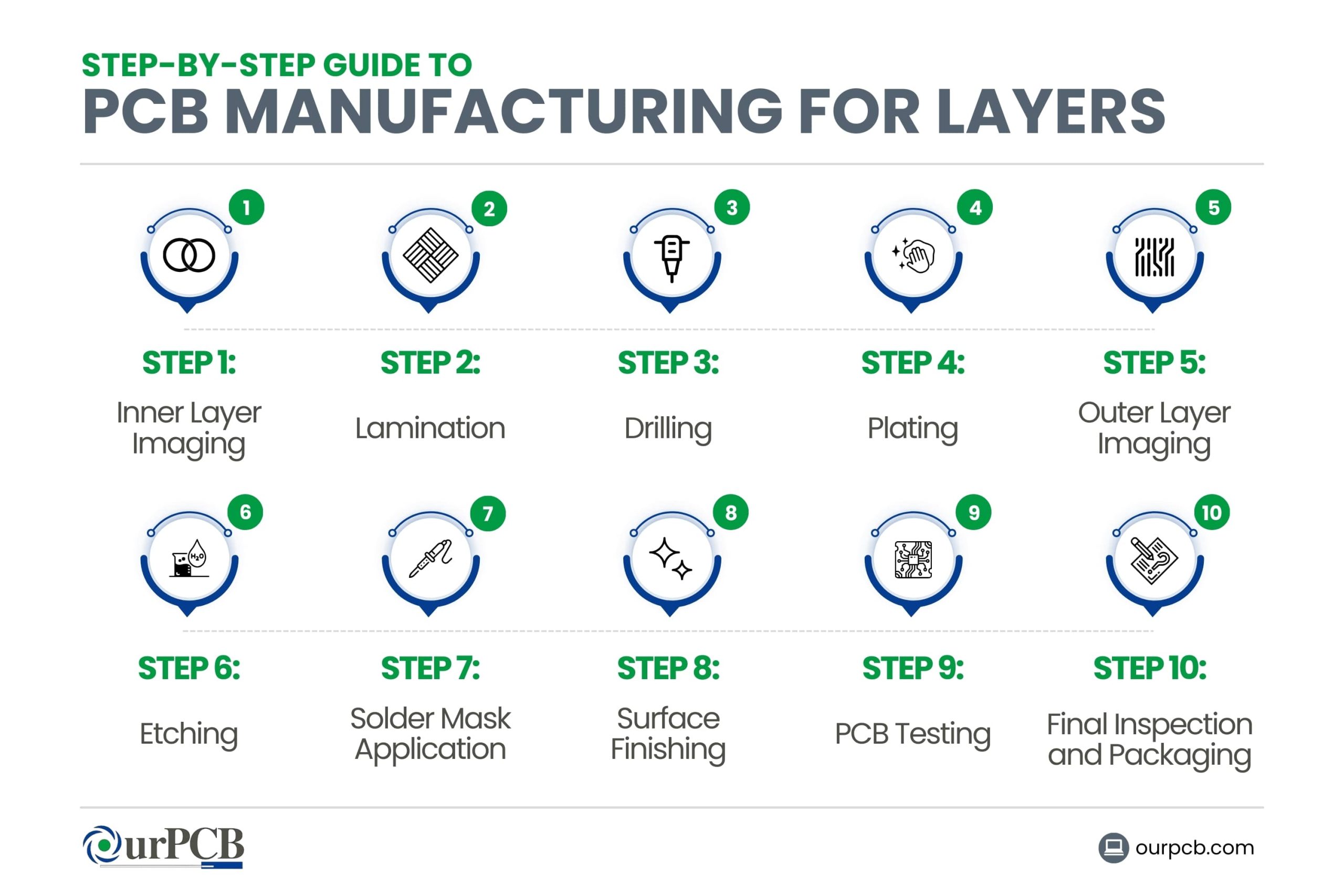
Step-by-Step Guide to PCB Manufacturing for Layers
-
Inner Layer Imaging
The inner layers of a PCB include the conducting copper foils that lay in the interior of its layers. Imaging, in this case, is printing the circuit image into the copper layers using UV light. The copper foils have photosensitive features, which is critical in enabling this process.
The imaging process requires sophisticated equipment in a controlled environment. Among this equipment is the fabrication system responsible for holding the copper laminate during the subsequent process. Others include exposure equipment, conveyorized developers, etchers and stripping equipment.
-
Lamination
Lamination of PCB layers involves pressing them together using intense pressure and heat. There’s usually a pair of hot plates, and the PCB layers are placed in between for compressing. This step is essential to ensure a perfect joinery without air in between.
-
Drilling
The manufacturer detects the slots for drilling using an X-ray machine. Next, the manufacturer drills the guiding slots and holes using a computer-controlled drill. The drilling process produces copper leftovers at the edges of the drill holes. These are removed via filing to ensure a clean PCB.
-
Plating
The manufacturer starts by cleaning the PCB and ensuring no residue on it. Next, the PCB is placed in a bath of chemicals to allow plating with a copper layer. The copper covers the holes left by the drilling process, which is handy for enhancing their electrical conductivity. This process yields Plated-Through Holes (PTH).
-
Outer Layer Imaging
This step involves applying a photoresist layer on the outer part of the PCB. Next, the manufacturer images the outer layers and then plates the PCB like in the previous step. The plating, in this case, involves applying a tin film. It helps shield the copper on the outer layers from damage.
-
Etching
Once the tin layer has been applied, some patches of unwanted copper will be on the outer part of the PCB. Removing this copper is where the etching process comes in handy. The manufacturer applies a copper solvent to dissolve the unwanted copper.
-
Solder Mask Application
The manufacturer thoroughly cleans the PCB to prepare the surface for solder mask application. Then, the manufacturer will apply an ink epoxy and a solder mask film. The solder mask protects the copper layer and discourages solder shorting during parts installation.
At this point, removing some parts of the solder mask is imperative. This is where UV light comes in handy, as it helps identify the areas where the removal is necessary. The next step is curing the solder mask in intense heat to create an efficient cover.
-
Surface Finish Application and Silkscreen Printing
This is where the manufacturer applies silkscreen with information such as the hole numbers, logo, and warning labels. Also, the PCB is inspected for efficient solder mask application to ensure there’s no excess solder.
The manufacturer will then apply surface finish materials that enhance conductivity and lower oxidation, such as:
- Hard gold
- Immersion silver
- Organic solderability preservative (OSP)
- Hot air solder leveling (HASL)
- Electroless nickel electroless palladium immersion gold (ENEPIG)
-
PCB Testing
One of the most common tests done on the PCB is the Electrical Reliability Test. It confirms that the PCB can conduct effectively. The other test is called the “bed of nails” test, which confirms the capacity of the PCB to withstand strenuous pressure.
-
Final Inspection and Packaging
Finally, the manufacturer inspects the PCB for aspects such as :
- Whether the holes are uniform and match the manufacturer's standards.
- If the circuit boards are clean from dust and other materials that could affect their integrity.
- Whether the boards have sharp edges that require filing before release to the market.
What are Flexible and Rigid-Flex PCBs?
From simple observation, you can tell if a PCB is either a flexible or rigid-flex. When a PCB is flexible, the entire conducting part can bend without the risk of breakage. On the flip side, a rigid-flex PCB is a mix of a flexible and a rigid PCB. Although it can move slightly, its flexibility is not as profound as that of a flexible PCB.
Flexible PCBs are popular in militaryware and fitness wearables due to their flexibility. They’re also popular in devices like cameras and smartphones, with the aim of having a small form factor device with complex features. Conversely, rigid-flex PCBs are applicable where flexibility is not a core necessity.
What Materials are Used in PCBs?
You can’t just use any material for PCB manufacturing as material significantly impacts the circuit board’s functioning. low volume electronics assembly will result in poor performance and short-term service.
Below are some of the best quality PCB materials and their fundamental properties.
Substrates
- FR-4: Glass-reinforced epoxy laminate (FR-4) is the most popular substrate option in PCB manufacturing. This is primarily because it exhibits excellent heat resistance and electrical insulation.
- Polyimide: Although Polyimide is less popular than FR-4, it's still a valid substrate option, especially when dealing with high-temperature applications. Its other upside is its flexibility, which makes it ideal for automobile and aerospace industry PCBs.
- Rogers: This is synonymous with a relatively low dielectric loss, making it the perfect fit substrate in high-frequency applications. Rogers substrate is helpful in radio frequency (RF) applications and other frequency circuits like microwave systems.
Conductive Materials
- Copper: Copper is undoubtedly the most popular conducting material thanks to its excellent conductivity and availability. Its cardinal role in PCB manufacturing is to create current flow pathways for a circuit. Copper’s effectiveness in electrical conductivity relies on thickness; the thicker it is, the better it becomes in conducting current.
- Aluminum: It’is less popular than copper but makes an excellent PCB conductive material, especially where heat dissipation is a crucial concern. One of its popular applications is in LED PCBs, where it helps release heat, helping the system conserve energy.
Insulating Materials
The primary insulating materials in PCBs are prepreg and core, lined up as sheets between the conducting layers. Prepreg is made of partially cured epoxy fiberglass, and it’s an excellent insulator. On the other hand, fully cured laminate makes up the core.
When the two are in a PCB, they help it gain good structural integrity while also acting as an insulator.
PCB Layers FAQs
What is the Difference Between 4-Layer and 6-Layer PCB?
A 4-layer PCB consists of two signal layers and the top/bottom layers, while a 6-layer PCB is a 4-layer PCB with two additional signal layers. The advantage of the 6-layer PCB over the 4-layer is that the former has an additional platform for routing signals. It can accommodate more components and is more suited to complex applications.
How Many Layers can a PCB Have?
The simplest PCB is a single layer, but it can have as many layers as possible, depending on the customer's requirements and the PCB's intended application. Multilayers can go up to 64 for the most sophisticated circuit boards.
How are PCB Layers Held Together?
PCB layers are enjoined via intense heat and pressure to ensure a solid uniform joint.
Final Thoughts
A clear grasp of PCB layers and how their constitution affects the board's functionality is a significant step in understanding the manufacturing process.
At OurPCB, we devote ourselves to manufacturing top-grade PCBs and are always ready to fulfil your demands, however many layers you want on your board. Our seasoned engineers will respond to your needs and fulfil your order within days.
Back to top: What Are Printed Circuit Board (PCB) Layers?
Special Offer: Get $100 off your order!
Email [email protected] to get started!