An 8-layer PCB stackup is a commonly used PCB design for electronic devices. Printed circuit boards (PCBs) are used in every electronic device. PCBs can be created with just one layer (the simplest designs) or up to 12 layers (found in some smartphones).
But what is an 8-layer PCB stackup exactly, and why is it a better choice than others? Ultimately, 8-layer PCB stackups offer more functionality and better performance than simpler PCBs like 4-layer stackup and 6-layer stackup designs, while not being overly complex. Here’s a deep dive into 8-layer PCB designs.
Contents
- What is an 8-Layer PCB Stackup?
- How is the 8-Layer PCB Stackup Configured?
- Examples of 8-Layer PCB Stackup Arrangements
- Example 1
- Example 2
- Example 3
- What Materials are Used in an 8-Layer PCB Stackup?
- Substrate Materials
- Prepreg
- Copper Foil
- Solder Mask
- Silkscreen
- Surface Finishes
- How Thick is an 8-Layer PCB Stackup?
- Key Factors Influencing Thickness
- Design Considerations for 8-Layer PCBs
- Signal Integrity
- Power Distribution
- Thermal Management
- Impedance Control
- Electromagnetic Compatibility (EMC)
- Routing and Trace Width
- Via Design
- Design Tools and Software
- Manufacturing Process of 8-Layer PCBs
- Guidelines for a Standard 8-Layer PCB Stackup
- Impedance Control
- Layer Separation
- Signal Shielding
- Ground Planes
- Balanced Layer Distribution
- Routing Direction
- Return Path
- Buried or Blind Vias
- Benefits of an 8-Layer PCB Stackup
- Improved Signal Integrity
- Reduced EMI
- Improved Ground and Power Plane Separation
- Enhanced High-Speed Signal Routing
- Minimized Crosstalk
- Lower Signal Loss
- Higher Component Density
- Increased Routing Space
- Better Thermal Management
- Challenges of an 8-Layer PCB Stackup
- When Should You Consider Using an 8-Layer PCB Stackup?
- Industries and Applications for 8-Layer PCBS
- Automotive Industry
- Consumer Electronics
- Medical Devices
- How Do you Design for Manufacturing (DFM) in an 8-Layer PCB?
- 8-Layer PCB Stackup FAQs
- How does an 8-Layer Stackup Differ from 4-Layer or 6-Layer PCBs?
- What Types of Motherboards Typically Use 8-Layer PCBs?
What is an 8-Layer PCB Stackup?
An 8-layer PCB stackup is a printed circuit board consisting of 8 different layers. These kinds of PC boards come in various configurations, but they usually have 4 signal layers and 4 plane layers. The signal layers are separated by the plane layers (ground and power planes), which helps to distribute power effectively across the board.
This kind of multilayer PCB design allows for complex routing paths without compromising performance, making it ideal for electronic devices that need high-speed performance in a compact package.
How is the 8-Layer PCB Stackup Configured?
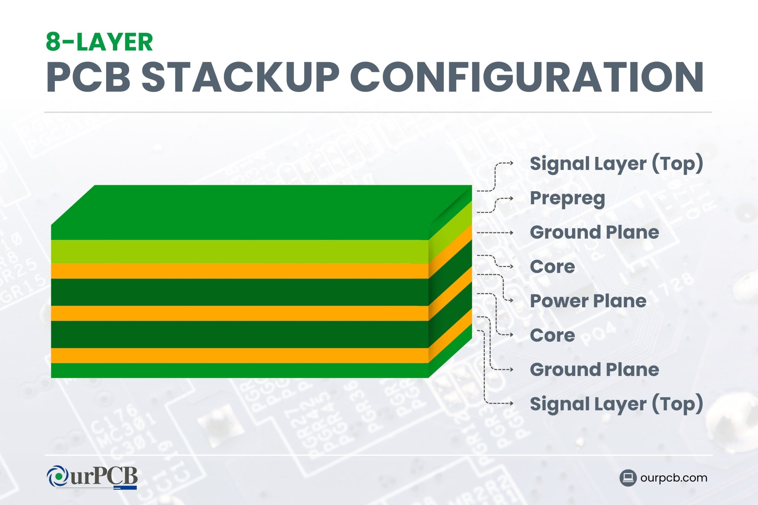
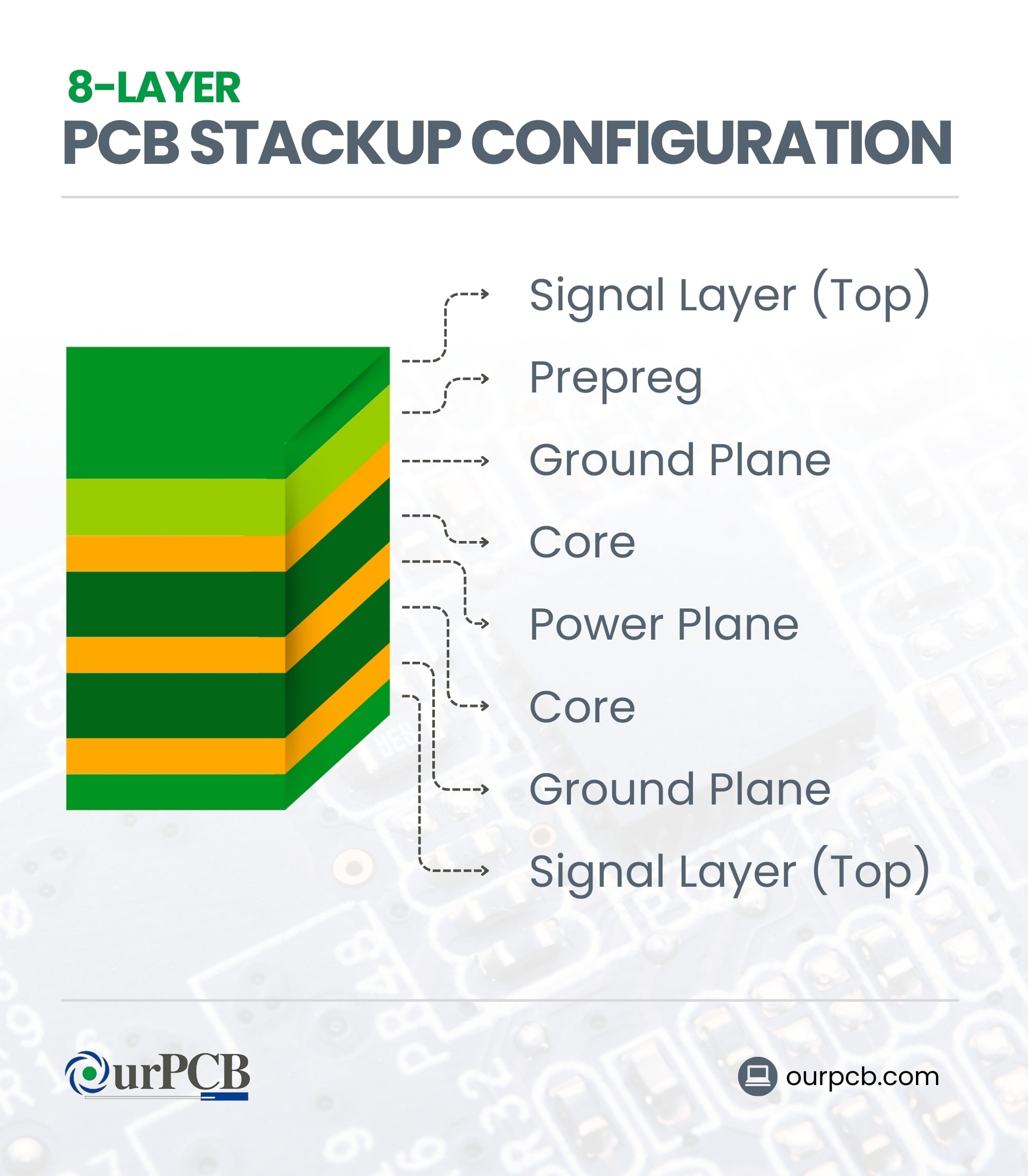
- Signal Layer (Top): The outermost PCB layer, often used for placing components, routing signals, and adding test points for easier debugging.
- Prepreg: A thin sheet of fiberglass cloth pre-impregnated with resin. This acts as the glue, bonding copper layers to the core during the lamination process.
- Ground Plane: A continuous layer of copper that provides a stable reference voltage for signals and helps to lower electromagnetic interference (EMI).
- Core: A thicker layer of fiberglass, typically FR-4, with copper cladding on both sides. It adds mechanical strength to the board.
- Power Plane: Similar to the ground plane, but dedicated to distributing power throughout the PCB. The internal power layer helps maintain a consistent voltage level and reduces noise in power delivery.
- Core: A second core layer provides additional rigidity and thickness to the PCB, further enhancing its mechanical properties.
- Ground Plane: Another ground plane layer is added for improved noise suppression and better signal referencing, especially for high-speed signals.
- Signal Layer (Bottom): The bottom layer mirrors the top layer’s function. It is used for routing signals, placing components, and providing access points for testing and soldering
Examples of 8-Layer PCB Stackup Arrangements
Example 1
In this type of PCB stackup design, the power and ground plane are coupled together in the center of the stackup. This kind of configuration allows for superb signal integrity. The outer ground layers shield the signal layers from each other, reducing crosstalk quite significantly.
- Signal 1
- Ground
- Signal 2
- Ground
- Power
- Signal
- Ground
- Signal 4
Example 2
This type of PCB stack places 2 signal layers in the center, sandwiched between the power and ground plane, for effective shielding from other signal layers and external EMI. The dual ground planes reduce ground impedance and improve performance.
- Signal 1
- Ground
- Power
- Signal 2
- Signal 3
- Ground
- Power
- Signal 4
Example 3
This type of 8-layer stackup uses ground planes as both the top and bottom layer, as well as an extra ground layer within the stack. This is effective for shielding the inner signal layer and minimizing crosstalk. All routing layers fall between the ground planes, creating a more predictable and consistent path for the return current.
- Ground
- Signal 1
- Ground
- Signal 2
- Signal 3
- Power
- Signal 4
- Ground
What Materials are Used in an 8-Layer PCB Stackup?
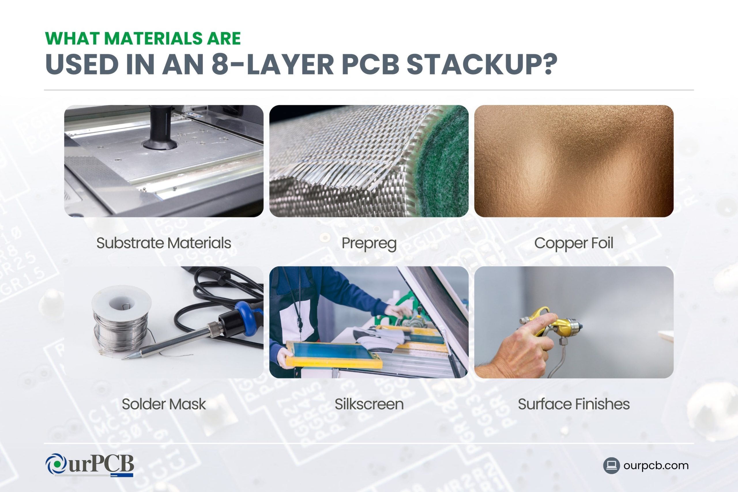
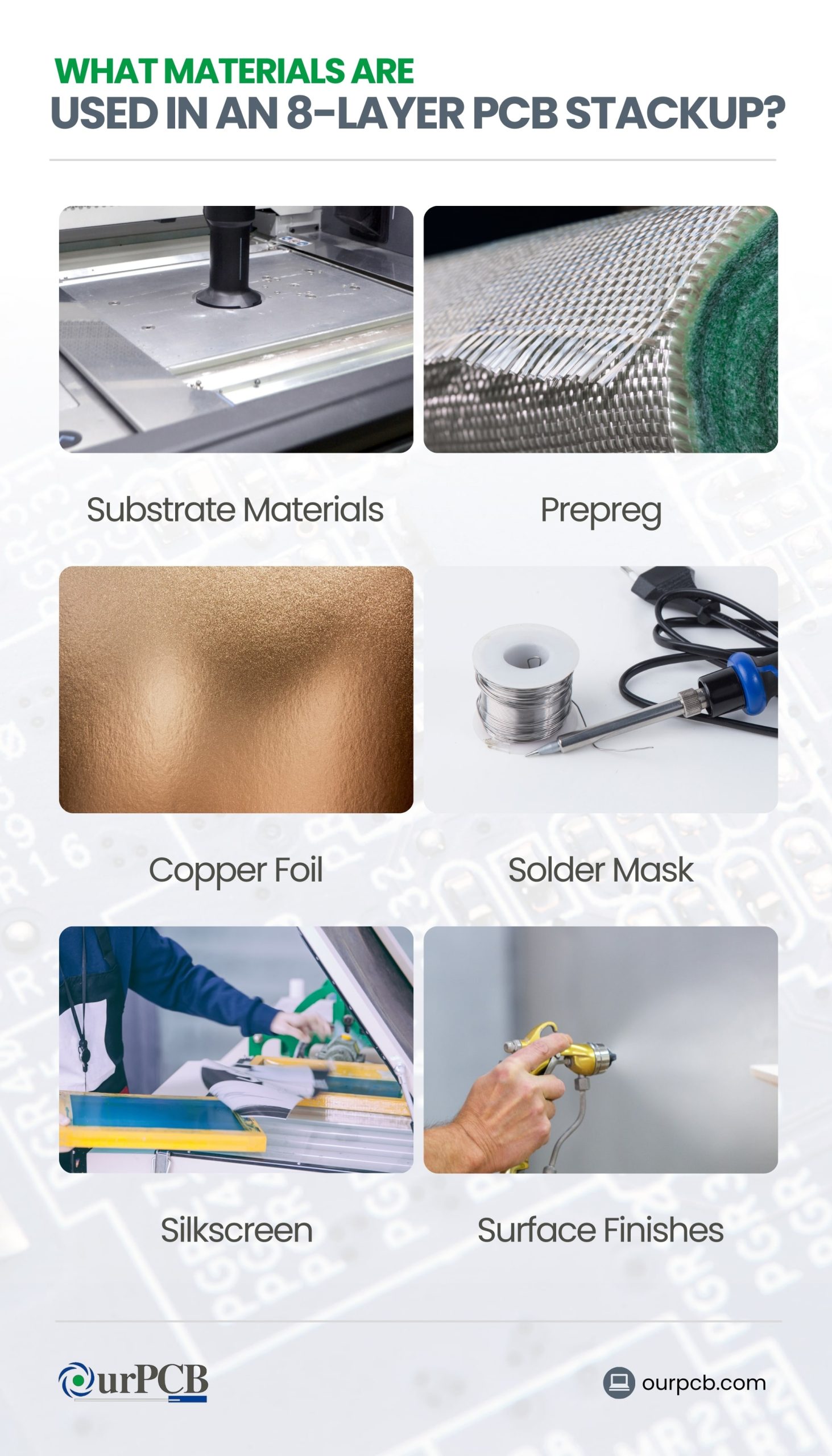
Substrate Materials
FR-4
FR-4 is a popular substrate material made from woven fiberglass cloth and epoxy resin. It offers good electrical insulation, mechanical strength, EMC performance, and thermal stability, making it suitable for a wide range of applications.
Polyimide
Polyimide substrates are used in high-performance 8-layer PCBs due to their superior temperature resistance and flexibility. They are ideal for applications where the board must endure extreme temperatures or require flexible circuits, adding versatility to the stackup.
Rogers Materials
Rogers materials are chosen for 8-layer PCBs that operate at high frequencies, such as RF and microwave applications. These PCB materials offer low dielectric loss and excellent electrical properties, ensuring signal integrity and reliability in complex multilayer designs.
Prepreg
Fiberglass Fabric
Fiberglass fabric in prepreg layers bonds the multiple layers in an 8-layer PCB. It reinforces the structure, providing stability and electrical insulation. The fiberglass fabric, impregnated with resin, keeps the layers securely bonded together.
Resin Systems
Resin systems in prepreg materials, such as epoxy, provide the necessary adhesion between layers. This helps maintain thermal stability and electrical insulation, both of which are essential for the board’s reliability.
Copper Foil
Electrodeposited Copper Foil
Electrodeposited copper foil (ED copper foil) is widely used in 8-layer PCB layouts because of its excellent conductivity and smooth surface. It forms the conductive pathways for electrical signals, ensuring efficient performance across all layers of the PCB.
Rolled Annealed Copper Foil
Rolled annealed copper foil is selected for 8-layer PCBs that need flexibility and durability. It’s ideal for applications involving mechanical stress or bending, providing reliable conductive paths without compromising the board’s integrity.
Solder Mask
LPI (Liquid Photoimageable) Solder Mask
LPI solder mask is commonly used in 8-layer PCBs to protect copper traces from oxidation and prevent solder bridges. This liquid coating is precisely applied and cured, which makes the PCB board highly reliable and protects the intricate multilayer circuitry.
Dry Film Solder Mask
Dry film solder mask is used in high-precision 8-layer PCBs. It provides exceptional protection for copper traces and is laminated onto the PCB for precise coverage and durability.
Silkscreen
Epoxy Ink
Epoxy ink is used for silkscreen printing on 8-layer PCBs to label components and provide important information. It’s durable and resistant to environmental factors, so labels remain legible throughout the board’s lifecycle.
Surface Finishes
Hot Air Solder Leveling (HASL)
HASL is a common surface finish in 8-layer PCB fabrication. The PCB is coated with molten solder and leveled with hot air. This provides a reliable solderable surface and protects the copper layers from oxidation.
Electroless Nickel Immersion Gold (ENIG)
ENIG involves plating nickel and gold over the copper traces, which offers excellent corrosion resistance, flatness, and a long shelf life, and makes it suitable for critical applications.
Organic Solderability Preservative (OSP)
OSP is an environmentally friendly surface finish some PCB manufacturers use. It applies a thin organic layer to protect the copper and maintain solderability. Although it may not be as durable as other finishes, it’s cost-effective and easy to apply.
How Thick is an 8-Layer PCB Stackup?
The board thickness of an 8-layer PCB stackup typically ranges from 0.062 to 0.096 inches (1.57 to 2.44 mm). This range accommodates various material choices and design specifications.
Key Factors Influencing Thickness
Prepreg and Core Materials
Prepreg and core materials play a significant role in determining the overall thickness of the PCB stackup design. Prepreg is used to bond layers together, while core materials provide structural stability:
- Prepreg Thickness: Typically ranges from 0.1 to 0.2 mm per sheet
- Core Thickness: Usually ranges from 0.3 to 0.5 mm per layer
Copper Foil Thickness
The thickness of the copper foil used in each layer also adds to the overall PCB thickness. Standard copper thicknesses include:
- 0.5 oz/ft² (0.017 mm)
- 1 oz/ft² (0.035 mm)
- 2 oz/ft² (0.070 mm)
Design Considerations for 8-Layer PCBs
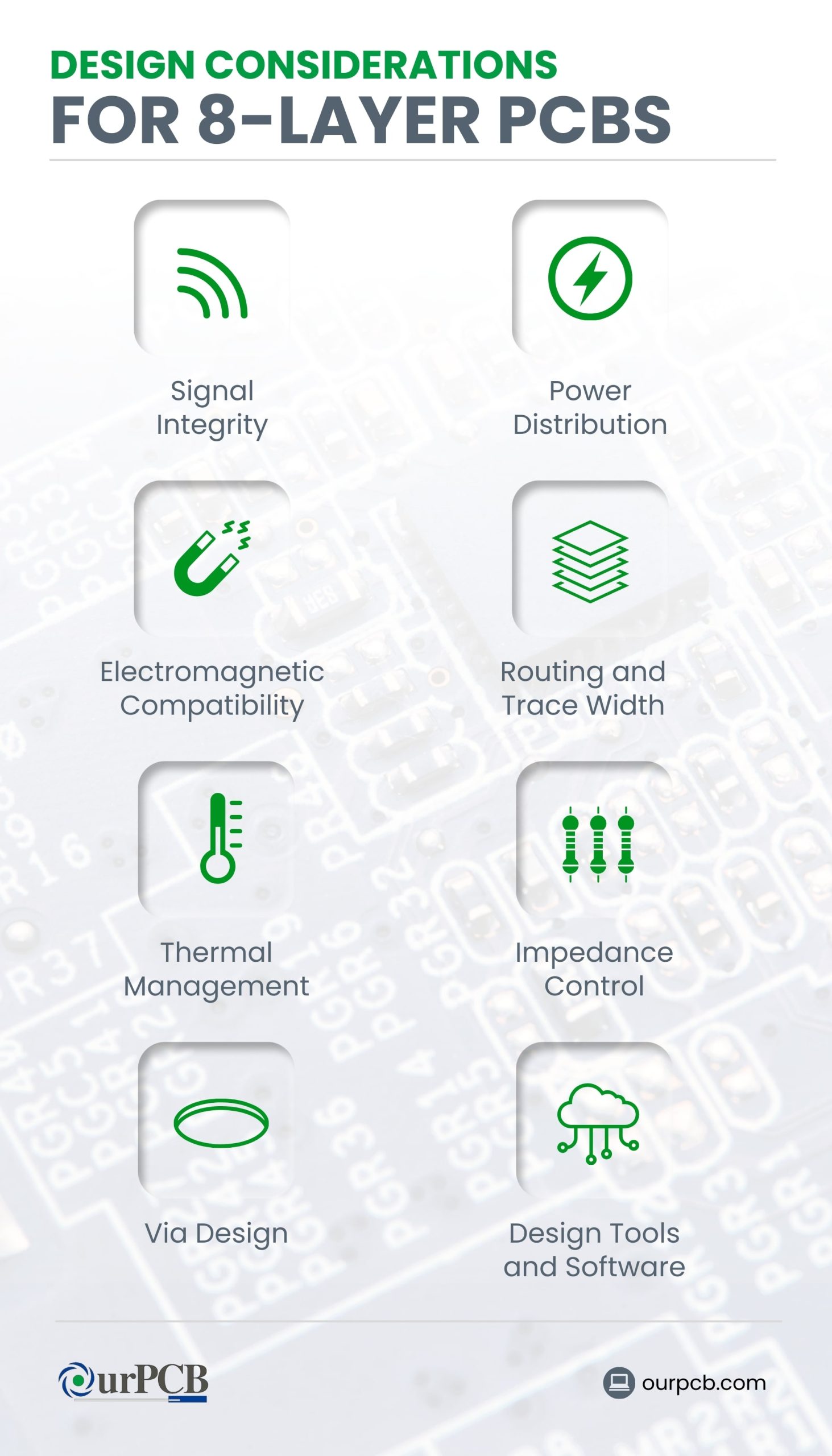
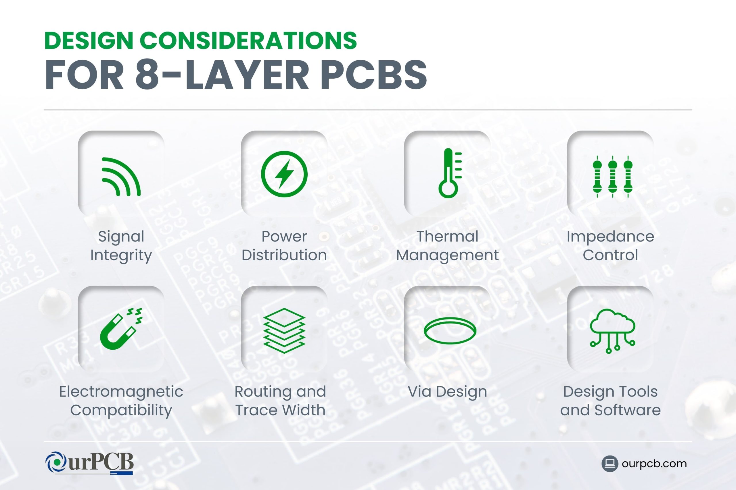
Signal Integrity
Excellent signal is a must in multilayer PCBs, especially in high-speed designs. Techniques to help signal travel without distortion include:
- Minimizing Crosstalk: Proper spacing between traces and using ground planes help reduce interference
- Controlled Impedance: Matching trace impedance to the transmission line requirements prevents signal reflections
Power Distribution
Efficient power distribution ensures all components of the PCB receive stable power. Power distribution is made possible by:
- Power Planes: Dedicated planes that distribute power evenly across the PCB
- Decoupling Capacitors: Placed near power pins of ICs to filter out noise and provide a stable voltage supply
Thermal Management
Overheating can make PCBs less reliable. Manage heat dissipation and keep circuits reliable by using:
- Thermal Vias: These transfer heat from hot components to other layers of the PCB, improving overall thermal performance.
- Heat Sinks: Attach heat sinks to high-power components to dissipate heat into the environment effectively. This helps maintain optimal operating temperatures for the components.
- Thermal Planes: Distribute thermal planes within the PCB layer stackup design to manage heat dissipation effectively. These planes help to spread the heat generated by components across a larger area, reducing hotspots.
Impedance Control
Controlling impedance will help your high-speed PCB maintain its fast signal transmission. Consider the following in your multilayer PCB stackups:
- Calculating Trace Width and Spacing: Based on the dielectric constant of the materials used
- Stackup Design: Proper layer arrangement helps achieve the desired impedance
Electromagnetic Compatibility (EMC)
EMC ensures a device doesn’t give off too much electromagnetic radiation and can handle interference from outside sources. Design ideas include:
- Shielding: Use ground planes and enclosures to reduce radiation
- Filtering: Use filters to get rid of unwanted frequencies
- Grounding: Good grounding techniques lower the risk of EMI problems
Routing and Trace Width
Careful routing and the right PCB trace width are important for signal integrity and reducing crosstalk:
- Differential Pairs: Routing high-speed signals in pairs helps to keep signal integrity up and decrease noise.
- Length Matching: Matching the lengths of traces in high-speed signals to keep the integrity of the signal and timing accuracy.
- Layer Stacking: Placing signal layers in the PCB layer stack in a smart way, often between ground or power planes, makes crosstalk and EMI less of a problem.
Via Design
Vias make electrical connections between layers. They can add inductance and capacitance, which affects signal integrity. Factors to think about include:
- Via Size: Pick the right via size based on the current-carrying capacity and signal frequency
- Via Types: Choose between through-hole, blind, and buried vias based on space and signal needs
- Antipad: Define the clearance area around the via to stop shorts to nearby copper features during the PCB manufacturing process
Design Tools and Software
Designing 8-layer PCBs requires special software tools. Both standard PCB designs and advanced PCB designs are created using:
- EDA Software: These software packages (Altium Designer, Cadence Allegro) help design schematics, lay out the PCB, and simulate signal behavior.
- Simulation Tools: Simulating signal behavior can identify possible signal or EMC problems before manufacturing.
Special Offer: Get $100 off your order!
Email [email protected] to get started!
Manufacturing Process of 8-Layer PCBs
- Design and Layout: Create a detailed schematic using the PCB stackup design guidelines and specialized software, laying out traces, vias, and components.
- Material Selection: Choose the right substrate material (typically FR-4), copper foil for conductive layers, and prepreg (a bonding material) for inner layers.
- Inner Layer Preparation: Etch away unwanted copper from copper-clad laminate to create the circuit pattern on inner layers.
- Layer Alignment and Bonding: Carefully align etched inner layers, prepreg, and copper foil for outer layers, then bond them together under heat and pressure (lamination).
- Drilling: Drill holes through laminated layers to create vias and component mounting holes.
- Plating: Plate the drilled holes with copper to create conductive pathways between layers.
- Outer Layer Preparation: Etch away unwanted copper from copper-clad laminate to create the final circuit pattern on outer layers.
- Solder Mask Application: Apply solder mask (usually green) to outer layers to protect copper traces and prevent solder bridges.
- Surface Finish: Apply a surface finish to exposed copper for protection and improved solderability.
- Silkscreen Printing: Print information like component designations on the PCB for easy identification during assembly.
- Electrical Testing: Conduct continuity and isolation tests to verify circuit functionality.
- Final Inspection and Quality Control: Perform visual inspection and additional tests to ensure the PCB meets specifications.
Guidelines for a Standard 8-Layer PCB Stackup
Impedance Control
Carefully pick trace widths and the distance between layers to ensure the signal flows smoothly and without distortion. This helps keep the signal strong and clear across the PCB.
Layer Separation
Think about the number of layers there are and how far apart the different layers should be. This helps make sure signals don't interfere with each other and makes the PCB work better overall.
Signal Shielding
Put important signal layers next to ground layers to protect them from outside noise and interference. This keeps the signals clean and reliable.
Ground Planes
Use solid ground planes whenever you can. These planes help to keep the electrical signals stable and make sure the whole PCB works well.
Balanced Layer Distribution
Spread out the signal, power, and ground layers evenly across the PCB. This helps with heat and signal flow, making the PCB more efficient.
Routing Direction
Route signals on different layers in different directions. This makes crosstalk (interference between signals) smaller and keeps the signals clear.
Return Path
Think about the path that the return current takes. This helps to make sure the signal has a good path back to its source, which is essential for signal quality.
Buried or Blind Vias
If you need more space for routing, think about using buried or blind vias. These vias only connect to some layers and can free up space on the surface.
Benefits of an 8-Layer PCB Stackup
Improved Signal Integrity
An 8-layer PCB stackup gives you consistent impedance control by precisely defining trace widths and spacings. This approach minimizes signal degradation and distortion, which is crucial for maintaining integrity in high-frequency applications.
Reduced EMI
Extra layers give you more space to spread out signals and protect them from interference. This makes sure that the PCB has cleaner signals and enhances overall circuit reliability.
Improved Ground and Power Plane Separation
The stackup provides dedicated layers for power and ground planes, optimizing power distribution and reducing noise in sensitive circuits. This separation enhances stability and reliability in high volume pcb manufacturing.
Enhanced High-Speed Signal Routing
By allowing controlled impedance routing, the 8-layer stackup minimizes transmission line effects such as reflections. This helps keep up the reliable transmission of high-speed signals that modern electronics rely on.
Minimized Crosstalk
By keeping signals on different layers and routing them in different directions, you can reduce the chance of signals interfering with each other (crosstalk). There should always be a separation between two signal layers.
Lower Signal Loss
Optimizing the PCB layer stackup reduces signal attenuation, maintaining signal strength over longer distances. This lowers signal loss for efficient transmission throughout the PCB.
Higher Component Density
With more layers available for routing and component placement, an 8-layer stackup allows for a more compact design. This facilitates higher component density, enabling the integration of complex functionalities into smaller PCB footprints.
Increased Routing Space
The additional layers provide more routing channels and vias, offering flexibility in design and accommodating complex interconnections without too much traffic along signal paths.
Better Thermal Management
Extra internal layers in the board stackup can be used for heat sinking and distribution. This improves thermal management by dissipating heat effectively, keeping the components running better for longer.
Challenges of an 8-Layer PCB Stackup
- Longer Lead Time: Making up a PCB board with 8 layers takes longer than simpler boards. There are more steps involved in making and putting together the different layers.
- Higher Manufacturing Costs: More layers mean more materials and more complicated processes, which drives up the cost to make the PCB. This might not be ideal for smaller projects with tight budgets.
- Testing Challenges: Checking for problems in an 8-layer PCB can be trickier than with simpler boards. The extra layers make it harder to see and fix any issues that might come up during testing.
- Limited Flexibility: Once you’ve made an 8-layer PCB, it’s not easy to change it. Adding or removing components can be difficult because of the way the layers are connected. This might not be great if you need to make changes later.
- Increased Weight: With more layers comes more weight. This might not be a big deal for some projects, but it can be a factor if you need to keep the overall weight down.
When Should You Consider Using an 8-Layer PCB Stackup?
- High-Speed Circuits: If you’re working with circuits that operate at high frequencies or speeds, an 8-layer stackup can help keep your signals clean and under control.
- Complex Designs: When your project has lots of parts and connections that need to be squeezed into a tight space, a higher layer count gives you the extra room to make it work.
- High-Density Interconnects (HDI): If you're working with small, intricate designs, 8 layers give you the space you need to make those tiny connections.
- Power Distribution Needs: When you need to get power to all parts of your board smoothly and efficiently, an 8-layer stackup gives you more options for power and ground planes.
- Compact Devices: If you’re making something small like a smartphone or medical device, 8 layers can help you fit everything in without sacrificing performance.
- Reliability Requirements: When your project needs to be tough and dependable, like in airplanes or cars, an 8-layer PCB can handle the stress.
- Signal Isolation: If you need to keep different signals from messing with each other, an 8-layer stackup gives you the layers you need to keep them separated.
- Prototype and Development: If you’re building a complex prototype and want to leave room for changes or improvements, an 8-layer PCB can give you that flexibility.
Industries and Applications for 8-Layer PCBS

Automotive Industry
- Advanced Driver Assistance Systems (ADAS): Collision avoidance systems and adaptive cruise control need complex circuits that 8-layer PCBs can handle much better than a 4-layer PCB can.
- In-Car Entertainment And Navigation Systems: With all the features packed into modern car electronics, 8-layer PCBs provide the space needed to connect everything.
Consumer Electronics
- High-End Audio Equipment: To get the best sound quality, audio gear needs precise and complex circuits, which often require an 8-layer PCB.
- Gaming Consoles: These powerful machines need a lot of processing power and memory, and 8-layer PCBs help them keep everything connected and running smoothly.
- Wearable Devices: Smartwatches, fitness trackers, and other wearables pack a lot of features into a tiny space, making 8-layer PCBs a good fit.
- Smart Home Devices: Thermostats, security systems, and other smart home gadgets often have complex circuits that control various functions, making 8-layer PCBs a good choice.
Medical Devices
- Imaging Systems: X-ray machines, MRI scanners, and other medical imaging devices need high-performance electronics to process complex images, often requiring 8-layer PCBs.
- Implantable Devices: Pacemakers, insulin pumps, and other devices implanted in the body need reliable and compact circuits, which 8-layer PCBs can provide.
- Diagnostic Equipment: Devices like EKG machines and blood glucose meters rely on precise electronics to measure and analyze medical data, often using 8-layer PCBs.
- Monitoring Devices: Wearable health monitors and other devices that track vital signs require compact and efficient circuits, which can be achieved with 8-layer PCBs.
How Do you Design for Manufacturing (DFM) in an 8-Layer PCB?
DFM in an 8-layer PCB includes optimizing the layer stackup to control impedance and keep the signal healthy. A well-designed PCB uses easy-to-manufacture trace widths and spacing, and strategically placing vias to simplify PCB assembly.
Clear documentation and rigorous design rule checks (DRC) are essential to streamline manufacturing processes and reduce errors during fabrication.
8-Layer PCB Stackup FAQs
How does an 8-Layer Stackup Differ from 4-Layer or 6-Layer PCBs?
An 8-layer PCB contains more layers than a 4- or 6-layer PCB. This allows for more room to route signals through the board, providing better performance and reliability than simpler PCB board designs.
What Types of Motherboards Typically Use 8-Layer PCBs?
High-end motherboards for gaming, intensive work like video editing, or other high-performance actions typically use 8-layer PCB stacks. This type of stack provides better capabilities to handle demanding functionalities.
Back to top: What is an 8-Layer PCB Stackup?
Special Offer: Get $100 off your order!
Email [email protected] to get started!