Contents
- Purpose and Significance of a Guard Ring in PCB Circuits
- How Guard Rings Work
- Electromagnetic Shielding
- Leakage Current Prevention
- Crosstalk Reduction
- Applications of Guard Rings in Sensitive Circuits
- Guard Ring Layout
- Thermocouple effect
- Guard Ring Placement
- PCB Guard Trace
- Capacitive Coupling and Crosstalk
- Guard Trace Purpose and Function
- PCB Guard Ring and EMI
- Understanding EMI in PCB Design
- Reducing EMI with Guard Traces
- What is PCB Ground Ring?
- PCB Ground Ring
- What is the Difference of Guard Ring VS Ground Ring?
Purpose and Significance of a Guard Ring in PCB Circuits
Guard rings play a critical role in maintaining circuit performance by reducing noise and interference in sensitive signal paths, such as clock signals or high-speed data lines. By providing a low-impedance path to ground, they act as a barrier against external noise, which is essential for achieving reliable operation in impedance control PCB designs. This ensures optimal performance in high-frequency or precision applications.
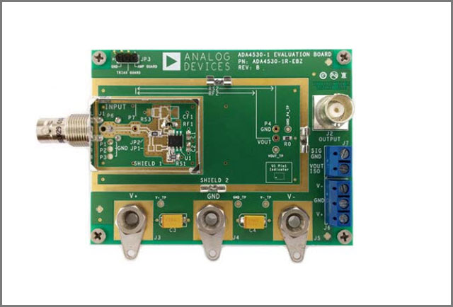 Image 1: PCB Guard Rings
Ensuring the current in the guard ring is equal to the current within the circuit, the potential difference is rendered zero and stops the wind from leaking.
How Guard Rings Work
Electromagnetic Shielding
Guard rings act as a Faraday cage, containing electromagnetic fields generated by signal traces. This containment reduces the likelihood of interference from nearby traces or components, ensuring the integrity of signals across the PCB.
Leakage Current Prevention
By providing a defined return path for stray currents, guard rings prevent leakage currents from affecting sensitive components. This controlled pathway helps maintain signal integrity and helps to reduce signal integrity problems in a PCB design, which is crucial in designing in designing effective PCB track transmission systems. This is especially important in high-precision applications where interference can compromise performance.
Crosstalk Reduction
Guard rings significantly reduce crosstalk when placed around signal traces. By increasing the distance between signal traces and adjacent components, they minimize capacitive coupling and unwanted signal interference.
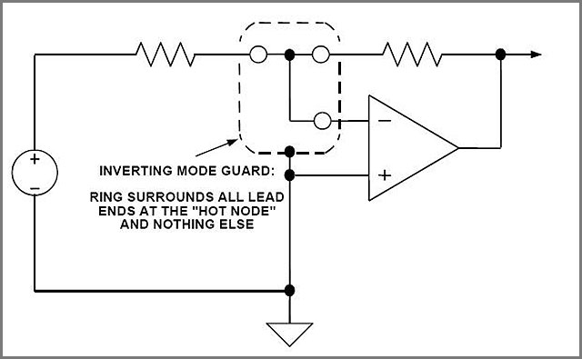 Image 2: PCB Guard Rings
Applications of Guard Rings in Sensitive Circuits
Guard rings are conductive traces or areas on PCBs designed to minimize noise, crosstalk, and leakage currents in sensitive circuits. They are commonly used in applications requiring high precision, such as electrocardiography (ECG), where even minor interference can compromise data accuracy.
While guard rings are not limited to AC circuits, they can be used in AC or DC systems to shield sensitive components and prevent interference or current leakage. In analog designs, the term "driven guard" is sometimes used to describe guard traces connected to a specific voltage potential to enhance performance further.
In ECG circuits and other precision systems, guard rings play a critical role in improving signal integrity by reducing leakage currents and preventing noise from impacting critical measurements.
Special Offer: Get $100 off your order!
Email [email protected] to get started!
Guard Ring Layout
The layout of a guard ring depends on its purpose and the type of circuit. For high-impedance AC analog circuits, specific factors must be considered when designing a guard ring.
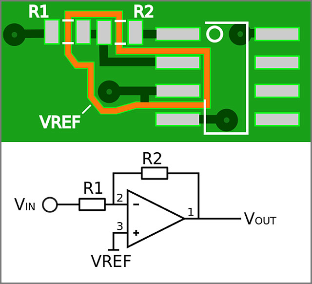 Image 3: Red Solder Mask
Thermocouple effect
To achieve precise readings, down to microvolts, the thermocouple effect must be accounted for. This effect occurs when two dissimilar metals form a thermoelectric junction, generating a small, temperature-dependent voltage. This phenomenon, also known as the "Seebeck Effect," is a common source of error in low-current measurement circuits.
Components like sockets, relay contacts, resistors, switches, and connectors can contribute to thermocouple errors. Even copper guard ring traces can create thermal EMFs of approximately 200 nV/°C, which can disrupt readings by about 2 nV.
To reduce thermocouple interference:
- Use components with minimal thermocouple effects. Some brands offer low thermal EMF options.
- Minimize the use of switches, sockets, and connectors. If unavoidable, select low-EMF versions.
- Carefully plan the layout to limit sources of thermal voltage generation.
Once the right components are chosen and the layout is optimized, the next step is proper placement of the guard rings.
Guard Ring Placement
Guard rings should be placed around the circuit’s input sections to minimize current leakage. This placement helps isolate sensitive areas and ensures more accurate readings.
The placement of guard rings depends on the configuration of the circuit:
- For inverting configurations, connect the guard ring to the positive input's potential.
- For noninverting configurations, connect the guard ring to the negative input's potential.
The correct placement reduces leakage current from input devices and improves measurement precision.
PCB Guard Trace
When designing a circuit with a guard ring to prevent current leakage and minimize thermal-induced EMF, one additional feature to enhance performance is the guard trace.
Guard traces are designed to reduce crosstalk in the circuit, making them an essential element in improving signal integrity. To understand the role of a guard trace, it’s helpful to first review crosstalk and capacitive coupling, the phenomena it addresses.
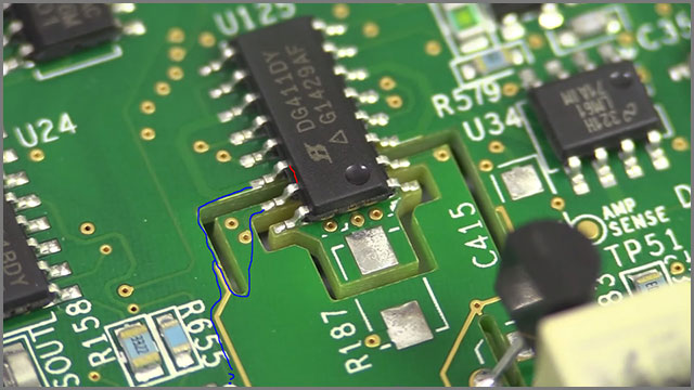 Image 4: PCB Guard Rings
Capacitive Coupling and Crosstalk
Capacitive Coupling
Capacitive coupling occurs when energy transfers between parts of a circuit through the displacement of current. In AC circuits, capacitive coupling blocks DC signals while allowing AC signals to pass. This interaction can have either intended or unintended effects on circuit performance.
Crosstalk
Crosstalk results from unintentional capacitive or inductive coupling between signal traces. It is a common issue in audio electronics, structured cabling, and integrated circuit designs. Crosstalk can lead to signal interference, degrading performance and causing noise in sensitive systems.
Guard Trace Purpose and Function
A guard trace is used to reduce or eliminate crosstalk in circuits. It is typically placed between parallel signal traces, acting as a barrier to block interference. Analog circuits often use guard traces, while they are less common in digital circuits. Even simple boards often include multiple guard traces to improve performance.
Key Components of a Guard Trace System:
- Aggressor Trace: The aggressor trace carries a signal and generates electromagnetic interference (EMI), which can affect nearby traces.
- Victim Trace: The victim trace is the signal path impacted by the EMI generated by the aggressor.
- Guard Trace: Positioned between the aggressor and victim traces, the guard trace reduces EMI and prevents crosstalk by creating an intermediate path for interference. It is connected to a stable voltage reference, such as VCC or ground.
Without a guard trace, crosstalk can significantly affect low-frequency signals, such as those in audio circuits. By adding a guard trace, signal interference is minimized, ensuring cleaner and more reliable circuit operation.
PCB Guard Ring and EMI
Electromagnetic interference (EMI) is a challenging issue to measure and resolve because nearly every component connected to a power source generates some level of interference, no matter how small. While minor interference might seem negligible, it can still impact circuit performance.
On a small scale, EMI can slow down a circuit or produce inaccurate results. On a larger scale, it can disrupt or even prevent the circuit from functioning entirely. This makes EMI an important consideration when designing a printed circuit board (PCB). Adhering to EMI design guidelines for EMI reduction is essential, particularly in RF PCB design, where effective EMI shielding is critical for reliable performance.
Understanding EMI in PCB Design
Each component in a circuit generates thermal and electromagnetic interference. These interferences can range from frequencies as low as 50 kHz, which may have minimal impact, to frequencies as high as 50 MHz, which can disrupt or shut down a circuit entirely. To effectively address EMI, you must evaluate all components and their potential contributions to interference.
One significant source of EMI is crosstalk, where unintentional coupling between signal traces introduces noise into the circuit. Crosstalk is a frequent issue that contributes to high levels of electromagnetic interference.
One significant source of EMI is crosstalk, where unintentional coupling between signal traces introduces noise into the circuit. Crosstalk is a frequent issue in high-frequency PCB designs, where managing interference is critical to ensuring reliable performance.
Reducing EMI with Guard Traces
Guard traces are an effective way to reduce EMI caused by crosstalk. By placing guard traces between signal lines, you create a barrier that helps isolate signals and reduces interference. While guard traces are primarily used to mitigate crosstalk, they also play an important role in minimizing EMI, helping to ensure stable circuit performance.
What is PCB Ground Ring?
PCB Ground Ring
- Purpose: A ground ring is primarily used for grounding purposes. It provides a continuous ground path around the edge of a PCB or specific circuit sections to improve grounding and reduce noise.
- Connection: Always tied to the ground plane of the PCB.
- Applications: Common in RF circuits, power electronics, or high-speed digital designs to ensure robust grounding and to act as an EMI shield.
- Example Use: In RF applications to reduce radiated EMI and improve return path integrity.
What is the Difference of Guard Ring VS Ground Ring?
While a PCB guard ring and ground ring have overlapping goals (e.g., reducing interference), they serve different purposes and are implemented differently. A guard ring is for protecting sensitive signals, while a ground ring is for establishing a stable ground connection and shielding against EMI.
Differences
| Feature | Guard Ring | Ground Ring |
|---|---|---|
| Primary Role | Prevent leakage and crosstalk. | Provide a robust ground path. |
| Connection | Low-impedance voltage or reference. | Always connected to the ground. |
| Use Case | Precision analog and signal circuits. | RF, power, and high-speed designs. |
Back to Top: What is a PCB Guard Ring?
Special Offer: Get $100 off your order!
Email [email protected] to get started!


